8182
LOW-DROPOUT,
3 V REGULATOR
DISCONTINUED PRODUCT
-- FOR REFERENCE ONL
Y
Designed specifically to meet the requirement for extended opera-
tion of battery-powered equipment such as cordless and cellular
telephones, the A8182SL voltage regulator offers the reduced dropout
voltage and quiescent current essential for maximum battery life.
Applicable also to palmtop computers and personal data assistants, the
device delivers a regulated 3 V output at up to 150 mA.
A PMOS pass element provides a typical dropout voltage of only
85 mV at 60 mA of load current. The low dropout voltage permits
deeper battery discharge before output regulation is lost. Furthermore,
quiescent current does not increase as the dropout voltage is
approached, an ideal feature in standby/resume power systems where
data integrity is crucial. Regulator accuracy and excellent temperature
characteristics are provided by a bandgap reference. An ENABLE input
and RESET output gives the designer complete control over power up,
standby, or power down.
This device is supplied in an 8-lead small-outline plastic package
(SOIC) for surface-mount applications. The A8182SL is rated for
operation over a temperature range of -20
∞
C to +85
∞
C.
FEATURES AND BENEFITS
s
High Efficiency Provides Extended Battery Life
s
85 mV Typical Dropout Voltage at I
O
= 60 mA
s
46
µ
A Typical Quiescent Current at V
I
= 6 V
Less than 1
µ
A "Sleep" Current
s
Up to 150 mA Output Current
s
CMOS-Compatible ON/OFF Control
For Power-Up, Standby, or Shutdown
s
Internal Thermal Protection
s
Surface-Mount Package
APPLICATIONS
s
Cordless and Cellular Telephones
s
Personal Data Assistants
s
Personal Communicators
s
Palmtop Computers
1
2
3
Dwg. PS-020
6
7
8
GND
RESET
COMP
OUT
IN
IN
ENABLE
OUT
VR
3 V
4
5
8182
Data Sheet
27468.2
PRELIMINARY INFORMATION DATA SHEET
(Subject to change without notice)
November 14, 1994
LOW-DROPOUT, 3 V REGULATOR
-- HIGH EFFICIENCY
Always order by complete part number:
A8182SL
.
ABSOLUTE MAXIMUM RATINGS
Input Voltage, V
I
. . . . . . . . . . . . . . 10 V
Output Current, I
O
. . . . . . . . . 150 mA*
Enable Input Voltage, V
E
. . . . . . . . . . V
I
Reset Output Voltage, V
OR
. . . . . . . . V
I
Reset Output Current, I
OR
. . . . 1.0 mA
Operating Temperature Range,
T
A
. . . . . . . . . . . . . -20
∞
C to +85
∞
C
Junction Temperature, T
J
. . . +150
∞
C
Storage Temperature Range,
T
S
. . . . . . . . . . . . -40
∞
C to +150
∞
C
* Output current rating is limited by input voltage,
duty cycle, and ambient temperature. Under any
set of conditions, do not exceed a junction temp-
erature of +150
∞
C. See next page.
Fault conditions that produce excessive junction
temperature will activate device thermal shutdown
circuitry. These conditions can be tolerated but
should be avoided.
8182
LOW-DROPOUT,
3 V REGULATOR
115 Northeast Cutoff, Box 15036
Worcester, Massachusetts 01615-0036 (508) 853-5000
MAXIMUM ALLOWABLE OUTPUT CURRENT with device mounted on 2.24" x 2.24"
(56.9 mm x 56.9 mm) solder-coated copper-clad board in still air.
Maximum Allowable Output Current in Milliamperes with V
I
= 8 V, T
J
= 150
∞
C, Period
10 s*
dc (Duty Cycle)
T
A
100%
90%
80%
70%
60%
50%
40%
30%
20%
25
∞
C
150
150
150
150
150
150
150
150
150
50
∞
C
150
150
150
150
150
150
150
150
150
70
∞
C
145
150
150
150
150
150
150
150
150
85
∞
C
120
130
150
150
150
150
150
150
150
* I
O
= (T
J
- T
A
)/([V
I
- V
O
] R
JA
∑ dc) = (150 - T
A
)/(5 ∑ 108 ∑ dc)
Output current rating can be increased (to 150 mA maximum) by heat sinking or reducing the input voltage. Conditions that produce excessive
junction temperature will activate device thermal shutdown circuitry. These conditions can be tolerated but should be avoided.
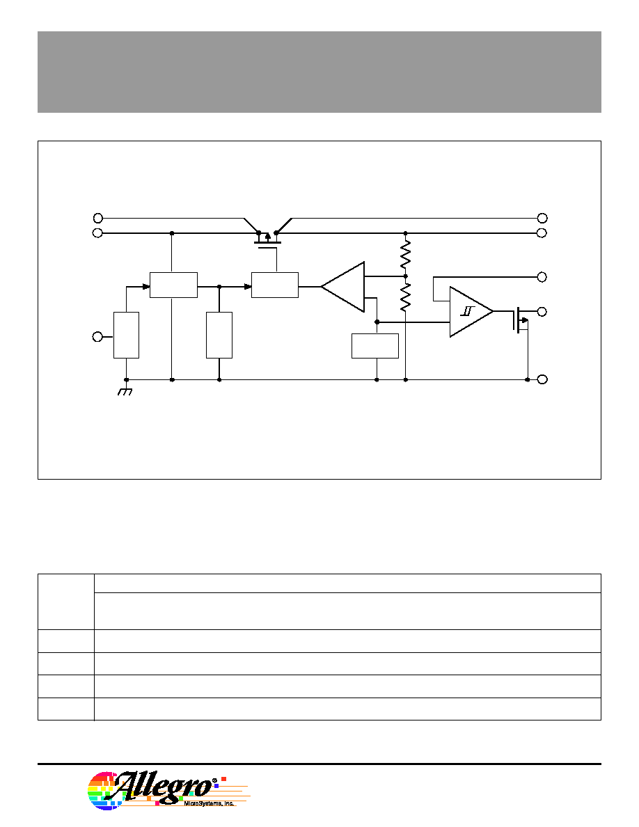
Dwg. FS-012-2
BIAS
DRIVE
ENABLE
THERMAL
PROTECT.
BANDGAP
REF.
ERROR
AMP
IN
ENABLE
OUT
IN
OUT
7
2
8
1
3
COMP
RESET
5
GND
4
6
1.23 V
≠
+
For proper operation, terminals 1 and 8 should be externally connected together,
terminals 2 and 7 should be externally connected together.
FUNCTIONAL BLOCK DIAGRAM
W
Copyright © 1994 Allegro MicroSystems, Inc.
8182
LOW-DROPOUT,
3 V REGULATOR
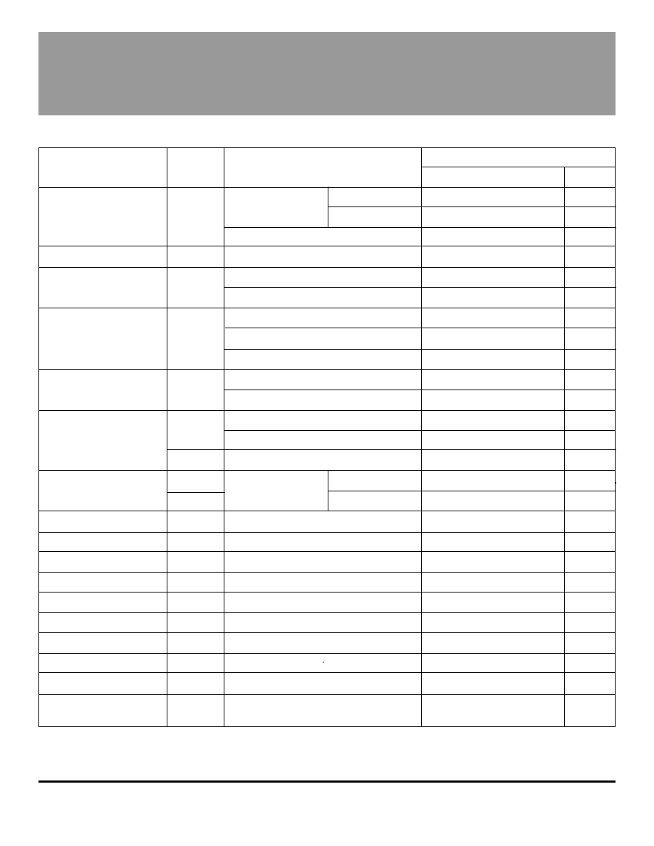
ELECTRICAL CHARACTERISTICS at T
A
= +25
∞
C (unless otherwise noted).
Limits
Characteristic
Symbol
Test Conditions
Min.
Typ.
Max.
Units
Output Voltage
V
O
4 V
V
I
8 V,
T
A
= +25
∞
C
2.95
3.00
3.05
V
10
µ
A
I
O
100 mA
-20
∞
C
T
A
+85
∞
C
2.90
3.00
3.10
V
V
I
= 3 V, I
O
= 60 mA, -20
∞
C
T
A
+85
∞
C
2.70
--
--
V
Output Volt. Temp. Coeff.
VO
V
I
= 6 V, I
O
= 10 mA
--
--
±
0.5
mV/
∞
C
Line Regulation
V
O(
VI)
6 V
V
I
8 V, I
O
= 1 mA
--
7.0
14
mV
4 V
V
I
6 V, I
O
= 1 mA
--
5.5
11
mV
Load Regulation
V
O(
IO)
1 mA
I
O
100 mA, V
I
= 8 V
--
12
30
mV
1 mA
I
O
100 mA, V
I
= 6 V
--
11
25
mV
1 mA
I
O
100 mA, V
I
= 4 V
--
8.0
20
mV
Dropout Voltage
V
I
min - V
O
I
O
= 60 mA
--
85
150
mV
I
O
= 125 mA*
--
175
TBD
mV
Quiescent Current
I
Q
V
I
= 6 V, 1 mA
I
O
100 mA, V
E
2.0 V
--
46
60
µ
A
(GND terminal current)
V
I
= 8 V, 1 mA
I
O
100 mA, V
E
2.0 V
--
50
65
µ
A
I
Q(off)
4 V
V
I
8 V, V
E
0.8 V
--
0.05
1.0
µ
A
ENABLE Input Voltage
V
EH
4 V
V
I
8 V,
Output ON
2.0
--
--
V
V
EL
-20
∞
C
T
A
+85
∞
C
Output OFF
--
--
0.8
V
ENABLE Input Current
I
E
T
A
+85
∞
C, V
E
= V
I
= 8 V
--
--
±
0.1
µ
A
COMP Threshold Voltage
V
C(t)
4 V
V
I
8 V, V
C
increasing from 0
1.20
1.23
1.30
V
COMP Threshold Volt. TC
VC
4 V
V
I
8 V
--
--
±
0.5
mV/
∞
C
COMP Threshold Hys.
V
C(hys)
4 V
V
I
8 V
12
34
50
mV
COMP Input Current
I
C
0 V
V
C
V
O
--
-25
TBD
nA
COMP Input Current TC
IC
4 V
V
I
8 V
--
-0.5
-2.5
nA/
∞
C
RESET Leakage Current
I
OR
V
OR
= V
I
= 10 V, T
A
= +85
∞
C
--
--
2.0
µ
A
RESET Output Voltage
V
OR
I
OR
= 500
µ
A
--
100
400
mV
Thermal Shutdown Temp.
T
J
150
--
--
∞
C
Thermal Resistance
R
JA
Mounted on 2.24" x 2.24" solder-coated
--
108
--
∞
C/W
copper-clad board in still air
Typical values are at T
A
= +25
∞
C and are given for circuit design information only.
* Pulse test (
50 ms). See previous page for duty cycle limitations.