8183
LOW-DROPOUT,
3 V REGULA-
TOR
DISCONTINUED PRODUCT
-- FOR REFERENCE ONL
Y
8183
Designed specifically to meet the requirement for extended opera-
tion of battery-powered equipment such as cordless and cellular
telephones, the A8183SLU voltage regulator offers the reduced dropout
voltage and quiescent current essential for maximum battery life.
Applicable also to palmtop computers and personal data assistants, the
device delivers a regulated, continuous 3 V output at up to 75 mA under
normal operating conditions, or to 150 mA (transient) under worst-case
conditions.
A PMOS pass element provides a typical dropout voltage of only
90 mV at 60 mA of load current. The low dropout voltage permits
deeper battery discharge before output regulation is lost. Furthermore,
quiescent current does not increase as the dropout voltage is ap-
proached, an ideal feature in standby/resume power systems where
data integrity is crucial. Regulator accuracy and excellent temperature
characteristics are provided by a bandgap reference. An ENABLE input
gives the designer complete control over power up, standby, or power
down.
This device is supplied in a 6-lead small-outline plastic package
(similar to the SOT-89/TO-243AA) for surface-mount applications. The
A8183SLU is rated for operation over a temperature range of -20
∞
C to
+85
∞
C.
FEATURES AND BENEFITS
s
High Efficiency Provides Extended Battery Life
s
90 mV Typical Dropout Voltage at I
O
= 60 mA
s
45
µ
A Typical Quiescent Current at V
I
= 6 V
Less Than 1
µ
A "Sleep" Current
s
Up to 150 mA Output Current
s
CMOS-Compatible ON/OFF Control
For Power-Up, Standby, or Shutdown
s
Internal Thermal Protection
s
Surface-Mount Package
APPLICATIONS
s
Cordless and Cellular Telephones
s
Personal Data Assistants
s
Personal Communicators
s
Palmtop Computers
Dwg. PS-021
VR
3 V
2
SUB
3
ENABLE
1
GND
6
OUT
SUB
IN
4
SUB
5
SUB
LOW-DROPOUT, 3 V REGULATOR
-- HIGH EFFICIENCY
Data Sheet
27468.4
ABSOLUTE MAXIMUM RATINGS
Input Voltage, V
I
. . . . . . . . . . . . . . 10 V
Output Current, I
O
. . . . . . . . . 150 mA*
Enable Input Voltage, V
E
. . . . . . . . . . V
I
Operating Temperature Range,
T
A
. . . . . . . . . . . . . -20
∞
C to +85
∞
C
Junction Temperature, T
J
. . . +150
∞
C
Storage Temperature Range,
T
S
. . . . . . . . . . . . -40
∞
C to +150
∞
C
* Output current rating is limited by input voltage,
duty cycle, and ambient temperature. Under
any set of conditions, do not exceed a junction
temperature of +150
∞
C. See next page.
Fault conditions that produce excessive junction
temperature will activate device thermal
shutdown circuitry. These conditions can be
tolerated but should be avoided.
Always order by complete part number:
A8183SLU
.
8183
LOW-DROPOUT,
3 V REGULATOR
115 Northeast Cutoff, Box 15036
Worcester, Massachusetts 01615-0036 (508) 853-5000
MAXIMUM ALLOWABLE OUTPUT CURRENT with device mounted on 2.24" x 2.24"
(56.9 mm x 56.9 mm) solder-coated copper-clad board in still air.
Maximum Allowable Output Current in Milliamperes with V
I
= 8 V, T
J
= 150
∞
C, Period
10 s*
dc (Duty Cycle)
T
A
100%
90%
80%
70%
60%
50%
40%
30%
20%
25
∞
C
95
105
120
135
150
150
150
150
150
50
∞
C
75
85
95
110
125
150
150
150
150
70
∞
C
60
65
75
85
100
120
150
150
150
85
∞
C
50
55
60
70
80
100
125
150
150
* I
O
= (T
J
- T
A
)/([V
I
- V
O
] R
JA
∑ dc) = (150 - T
A
)/(5 ∑ 258 ∑ dc)
Output current rating can be increased (to 150 mA maximum) by heat sinking or reducing the input voltage. Conditions that produce excessive
junction temperature will activate device thermal shutdown circuitry. These conditions can be tolerated but should be avoided.
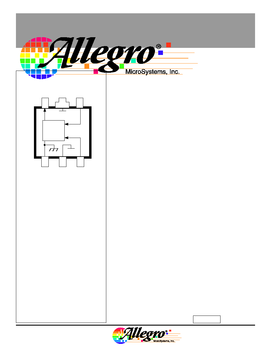
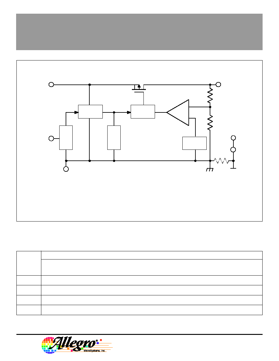
FUNCTIONAL BLOCK DIAGRAM
Dwg. FS-012-3
BIAS
DRIVE
ENABLE
THERMAL
PROTECT.
BANDGAP
REF.
ERROR
AMP
IN
ENABLE
OUT
4
6
3
2
1
5
GND
SUB
SUB
SUB
Terminal numbering is in accordance with EIA/JEDEC convention.
Where EIAJ conventions apply, the tab is not numbered, resulting in
terminal 6 being designated terminal 5.
For proper operation, terminals 1 and 2 must be externally con-
nected together.
W
Copyright © 1994 Allegro MicroSystems, Inc.
8183
LOW-DROPOUT,
3 V REGULA-
TOR
ELECTRICAL CHARACTERISTICS at T
A
= +25
∞
C (unless otherwise noted).
Limits
Characteristic
Symbol
Test Conditions
Min.
Typ.
Max.
Units
Output Voltage
V
O
4 V
V
I
8 V,
T
A
= +25
∞
C
2.95
3.00
3.05
V
10
µ
A
I
O
100 mA*
-20
∞
C
T
A
+85
∞
C
2.90
3.00
3.10
V
V
I
= 3 V, I
O
= 60 mA*, -20
∞
C
T
A
+85
∞
C
2.70
--
--
V
Output Volt. Temp. Coeff.
VO
V
I
= 6 V, I
O
= 10 mA
--
--
±
1.0
mV/
∞
C
Line Regulation
V
O(
VI)
6 V
V
I
8 V, I
O
= 1 mA
--
4.0
10
mV
4 V
V
I
6 V, I
O
= 1 mA
--
9.5
18
mV
Load Regulation
V
O(
IO)
1 mA
I
O
100 mA*, V
I
= 8 V
--
19
30
mV
1 mA
I
O
100 mA*, V
I
= 6 V
--
14
25
mV
1 mA
I
O
100 mA*, V
I
= 4 V
--
8.0
20
mV
Dropout Voltage
V
I
min - V
O
I
O
= 60 mA*
--
90
150
mV
I
O
= 125 mA*
--
190
300
mV
Quiescent Current
I
Q
V
I
= 6 V, 1 mA
I
O
100 mA*, V
E
2.0 V
--
45
60
µ
A
(GND terminal current)
V
I
= 8 V, 1 mA
I
O
100 mA*, V
E
2.0 V
--
50
65
µ
A
I
Q(off)
4 V
V
I
8 V, V
E
0.8 V
--
--
1.0
µ
A
ENABLE Input Voltage
V
EH
4 V
V
I
8 V,
Output ON
2.0
--
--
V
V
EL
-20
∞
C
T
A
+85
∞
C
Output OFF
--
--
0.8
V
ENABLE Input Current
I
E
T
A
+85
∞
C, V
E
= V
I
= 8 V
--
--
±
0.1
µ
A
Thermal Shutdown Temp.
T
J
150
--
--
∞
C
Thermal Resistance
R
JA
Mounted on 2.24" x 2.24" solder-coated
--
258
--
∞
C/W
copper-clad board in still air
Typical values are at T
A
= +25
∞
C and are given for circuit design information only.
* Pulse test (
20 ms). See previous page for duty cycle limitations.