DISCONTINUED PRODUCT
-- FOR REFERENCE ONLY
Designed specifically to meet the requirement for extended opera-
tion of battery-powered equipment such as cordless and cellular tele-
phones, the A8226SLM thru A8233SLM voltage regulators offer the
reduced dropout voltage and quiescent current essential for maximum
battery life. Applicable also to palmtop computers and personal data
assistants, these devices deliver a regulated output at up to 100 mA
(transient), which is limited only by package power dissipation. Regu-
lated output voltages of 2.6, 2.7, 2.8, 2.9, 3.0 and 3.3 are currently
provided. Other voltages, down to 2.0 volts, are available on special
order.
A PMOS pass element provides a typical dropout voltage of only
125 mV at 50 mA of load current. The low dropout voltage permits
deeper battery discharge before output regulation is lost. Quiescent
current does not increase significantly as the dropout voltage is ap-
proached, an ideal feature in standby/resume power systems where data
integrity is crucial. Regulator accuracy and excellent temperature
characteristics are provided by a bandgap reference. The A8226SLM
thru A8233SLM include ENABLE inputs to give the designer complete
control over power up, standby, or power down.
These devices are supplied in a thermally enhanced 5-lead small-
outline plastic package similar to the SOT-23, and fitting the SC-74A
footprint. All devices are rated for operation over a temperature range
of -20
∞C to +85∞C.
FEATURES AND BENEFITS
I High Efficiency Provides Extended Battery Life
I 125 mV Typical Dropout Voltage at I
O
= 50 mA
I 32 µA Typical Quiescent Current
Less Than 1
µA "Sleep" Current
I Low Output Noise
I 100 mA Peak Output Current
I Improved PSRR and Transient Performance
APPLICATIONS
I Cordless and Cellular Telephones
I Personal Data Assistants
I Personal Communicators
I Palmtop Computers
LOW-DROPOUT REGULATORS
-- HIGH EFFICIENCY
Data Sheet
27468.10
8226
THRU
8233
PRELIMINARY INFORMATION
(subject to change without notice)
January 18, 2000
A82xxSLM
Always order by complete part number, e.g., A82xxSLM , where "xx" is
the required output voltage in tenths.
ABSOLUTE MAXIMUM RATINGS
Input Voltage, V
I
. . . . . . . . . . . . . . . 7 V
Peak Output Current,
I
OM
. . . . . . . . . . . . . . . . . . 100 mA*
Enable Input Voltage, V
E
. . . . . . . . . . V
I
Operating Temperature Range,
T
A
. . . . . . . . . . . . . -20
∞
C to +85
∞
C
Junction Temperature, T
J
. . . . +150
∞
C
Storage Temperature Range,
T
S
. . . . . . . . . . . . -40
∞
C to +150
∞
C
* Output current rating is limited by input
voltage, duty cycle, and ambient temperature.
Under any set of conditions, do not exceed a
junction temperature of +150
∞C. See follow-
ing pages.
Dwg. PS-021-3
VR
2
GND
3
NO
CONNECT
1
ENABLE
5
IN
OUT
4
NC

8226
THRU
8233
LOW-DROPOUT
REGULATORS
115 Northeast Cutoff, Box 15036
Worcester, Massachusetts 01615-0036 (508) 853-5000
FUNCTIONAL BLOCK DIAGRAM
Copyright © 2000, Allegro MicroSystems, Inc.
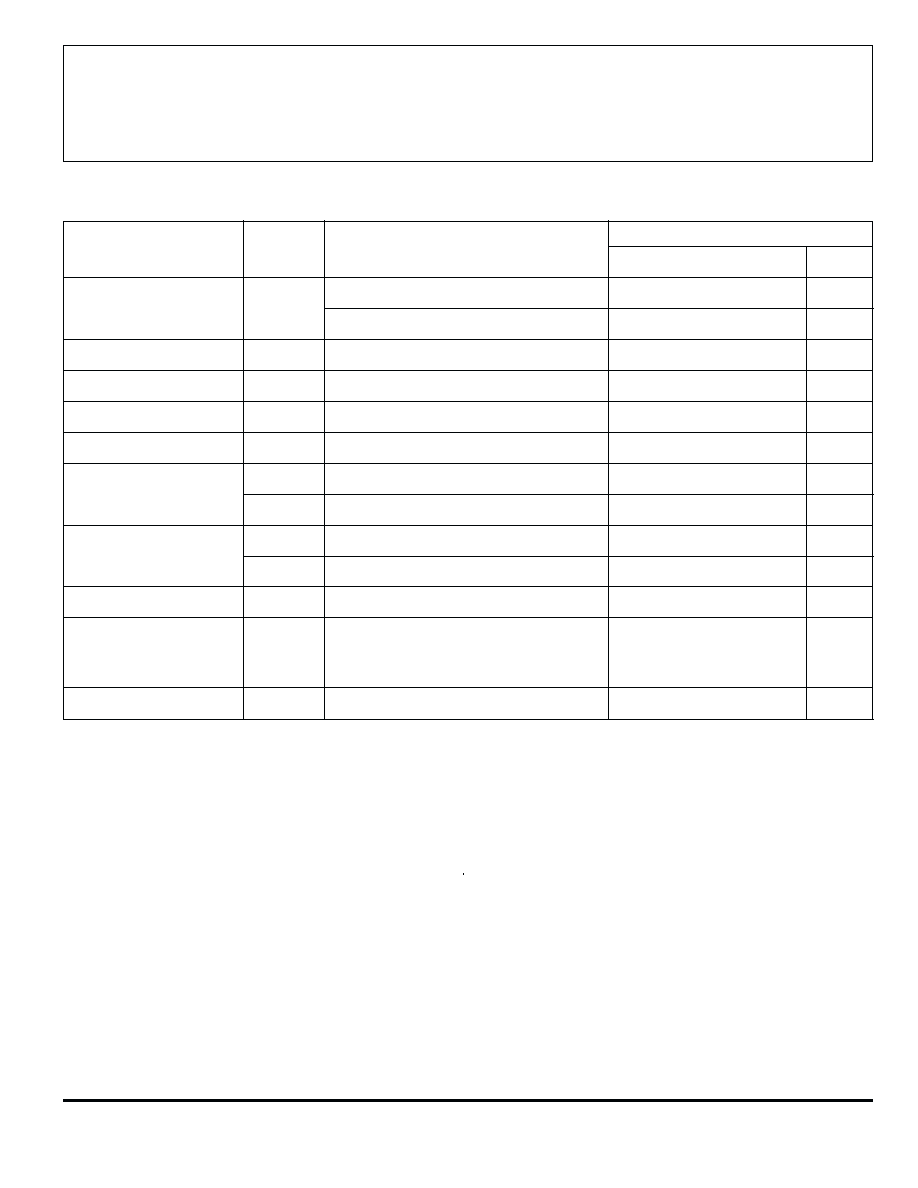
A82xxSLM Maximum Allowable Average Output Current* with device mounted on 2.24" x 2.24"
(56.9 mm x 56.9 mm) solder-coated copper-clad board in still air.
Allowable Total Average (10 ms) Output Current in Milliamperes with T
J
= 150
∞C, Duty Cycle = 100%
V
I
- V
O
T
A
1.5
2.0
2.5
3.0
3.5
4.0*
4.5*
25
∞C
100
100
100
100
100
100
100
50
∞C
100
100
100
100
100
100
100
70
∞C
100
100
100
100
100
91
81
85
∞C
100
100
100
98
84
74
66
* Absolute maximum peak output current rating is 100 mA; absolute maximum input voltage is 7 V.
I
O
= (T
J
≠ T
A
)/([V
I
≠ V
O
] R
JA
x dc) = (150 ≠ T
A
)/([V
I
≠ V
O
] x 220 x 1.00)
Output current rating can be increased (to 100 mA maximum) by additional heat sinking or reducing the duty cycle.
Dwg. FS-012-5B
BIAS
DRIVE
ENABLE
BANDGAP
REF.
ERROR
AMP
IN
ENABLE
OUT
5
4
1
2
GND
8226
THRU
8233
LOW-DROPOUT
REGULATORS
www.allegromicro.com
ELECTRICAL CHARACTERISTICS at T
A
= +25
∞C, V
E
2.0 V (unless otherwise noted).
Limits
Characteristic
Symbol
Test Conditions
Min.
Typ.
Max.
Units
Output Voltage
V
O
4 V
V
I
7 V, 10 µA I
O
50 mA*
-0.05
0.00
+0.05
V
(reference specified V
O(nom)
)
V
I
= V
O(nom)
, I
O
= 50 mA
--
--
-0.25
V
Output Volt. Temp. Coeff.
a
VO
V
I
= 6 V, I
O
= 10 mA, T
J
125∞C
--
-0.20
--
mV/
∞C
Line Regulation
V
O(
VI)
4 V
V
I
7 V, I
O
= 1 mA
--
3.0
10
mV
Load Regulation
V
O(
IO)
1 mA
I
O
50 mA*, 4 V V
I
7 V
--
--
20
mV
Dropout Voltage
V
I
min - V
O
I
O
= 50 mA
--
125
250
mV
Ground Terminal Current
I
GND
V
I
< 7 V, I
O
50 mA
--
32
45
µA
I
Q
V
I
7 V, V
E
0.8 V, I
O
= 0 mA
--
--
1.0
µA
ENABLE Input Voltage
V
EH
4 V
V
I
7 V, Output ON
2.0
--
--
V
V
EL
4 V
V
I
7 V, Output OFF
--
--
0.8
V
ENABLE Input Current
I
E
V
E
= V
I
= 7 V
--
--
±1.0
µA
Rejection Ratio
PSRR
V
I
= V
O(nom)
+ 1.5 V, V
i
= 100 mV, I
O
= 10 mA,
f = 1 kHz
--
70
--
dB
f = 10 kHz
--
52
--
dB
Output Noise
e
n
10 Hz
f 100 kHz, I
O
= 10 mA, C
O
= 10
µF
--
0.5
--
µV/Hz
Typical values are at T
A
= +25
∞C and are given for circuit design information only.
* Pulse test (
20 ms). See previous page for duty cycle limitations.