 | –≠–ª–µ–∫—Ç—Ä–æ–Ω–Ω—ã–π –∫–æ–º–ø–æ–Ω–µ–Ω—Ç: 8283 | –°–∫–∞—á–∞—Ç—å:  PDF PDF  ZIP ZIP |

Data
Sheet
27448
8283
LNB SUPPLY AND
CONTROL-VOLTAGE REGULATOR
Always order by complete part number, e.g., A8283SLB .
Intended for analog and digital satellite receivers, the low-noise block
converter regulator (LNBR) is a monolithic linear and switching voltage
regulator designed to provide power and interface signals to the LNB down
converter via the coaxial cable. If the device is in stand-by mode (EN terminal
LOW), the regulator output is disabled, allowing the antenna downconverters to
be supplied or controlled by other satellite receivers sharing the same coaxial
cable. Similar two-output LNB supply and control voltage regulators are the
A8284SB/SLB.
For slave operation in single-dish dual-receiver systems, the bypass
function is implemented by an electronic switch between the master input
terminal (MI) and the LNB terminal, leaving all LNB power and control
functions to the master receiver. This electronic switch is closed if the device
is powered, EN is HIGH, and OSEL is LOW.
The regulator outputs are set to 12, 13, 18, or 20 V by the VSEL terminals.
Additionally, it is possible to increase the selected voltage by 1 V to compen-
sate for the voltage drop in the coaxial cable (LLC terminal HIGH). The
LNBR combines a tracking switching regulator and low-noise linear regulator.
Logic inputs (VSEL0, VSEL1, and LLC) select the desired output voltage. A
tracking current-mode buck converter provides the linear regulator with an
input voltage that is set to the output voltage plus typically 0.8 V. This main-
tains constant voltage drop across the linear regulator while permitting ad-
equate voltage range for tone injection.
The device is supplied in a 24-pin plastic DIP with batwing tabs
(A8283SB), or a 24-lead SOIC power-tab package (A8283SLB). In both cases,
the power tab is at ground potential and needs no electrical isolation.
ABSOLUTE MAXIMUM RATINGS
Supply Voltage, V
IN
.......................... 47 V
Output Current, I
O
.... Internally Limited
Logic Input Voltage Range,
V
I
................................... -0.5 V to +7 V
Bypass Switch Current,
I
SW
........................ Internally Limited
Flag Output Voltage, V
OLF
.................. 7 V
Operating Temperature Range,
T
A
............................... -20
∞
C to +85
∞
C
Storage Temperature Range,
T
S
............................. -40
∞
C to +150
∞
C
FEATURES
I Short-Circuit Protected Bypass Function for Slave Operation
I LNB Selection and Stand-By Function
I Built-In Tone Oscillator Factory Trimmed to 22 kHz, Facilitates
DiSEqCTM (a trademark of EUTELSAT) Encoding
I Full Modulation With No Load
I Tracking Switch-Mode Power Converter for Lowest Dissipation
I Externally Adjustable Short-Circuit Protection
I LNB Short-Circuit Protection and Diagnostics
I Auxiliary Modulation Input
I Cable Length Compensation
I Internal Over-Temperature Protection
This device incorporates features that have patents pending.
PRELIMINARY INFORMATION
(Subject to change without notice)
November 21, 2000
23
17
8
1
2
3
4
5
6
7
9
12
16
14
13
24
22
21
20
19
18
11
10
9
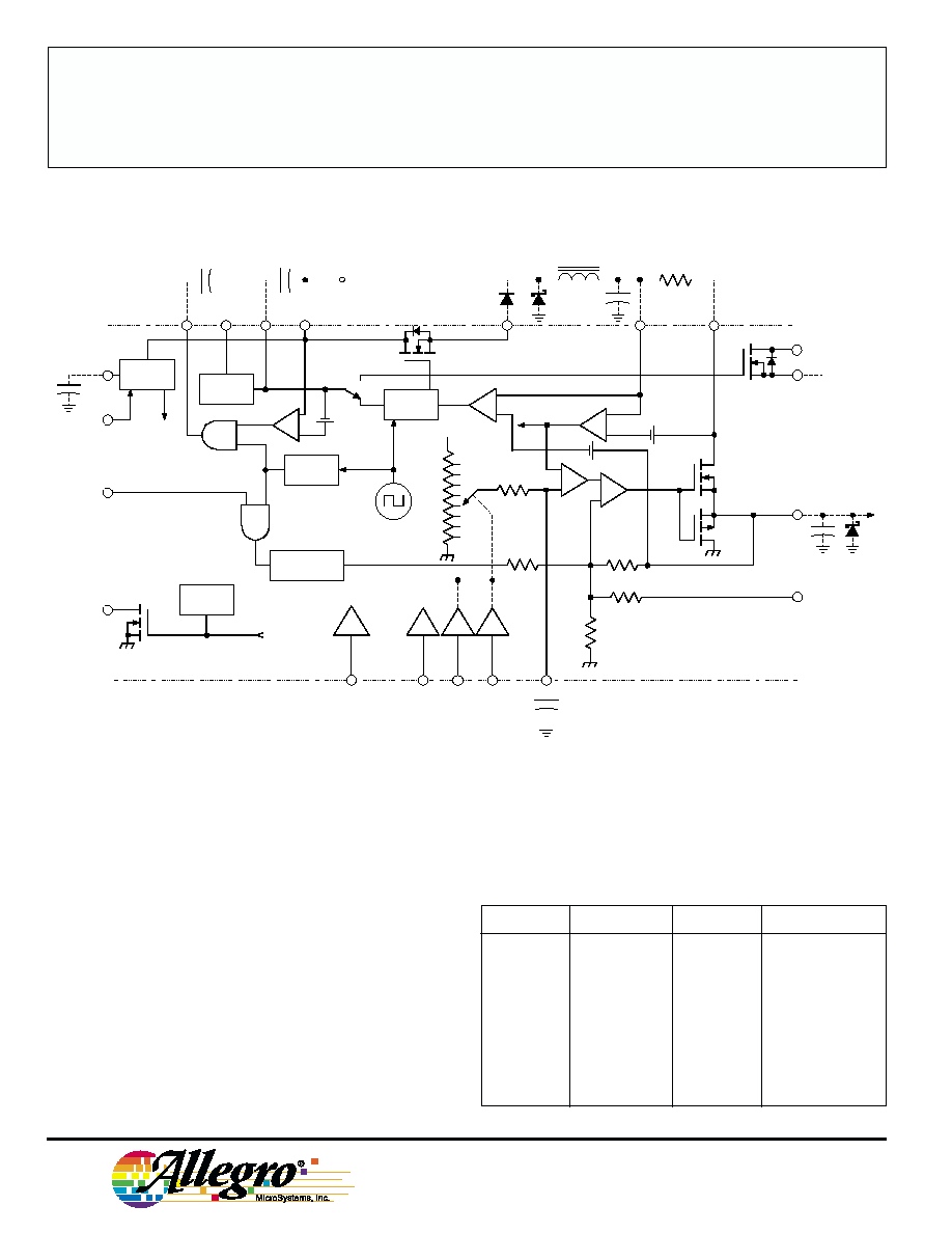
EXTM
VINT
PUMPX
VPUMP
CPUMP
GND
GND
ENT
EN
VSEL0
VSEL1
LLC
OSEL
OLF
VBULK
MIOUT
MI
GND
GND
SENSE
LNB
LX
VIN
TCAP
CHARGE
PUMP
VOLTAGE
CONTROL
REG.
BUCK
Dwg. PP-072A
15
Note that the A8283SB (dual in-line package)
and A8283SLB (small-outline IC package) are
electrically identical and share a common
terminal number assignment.
A8283SLB
8283
LNB SUPPLY AND
CONTROL-VOLTAGE REGULATOR
115 Northeast Cutoff, Box 15036
Worcester, Massachusetts 01615-0036 (508) 853-5000
2
VREF
OVER-
CURRENT
TSD
+
352 kHz
OVER-
CURRENT
RS
150 mV
800 mV
176 kHz
22 kHz TONE
ENT
PUMPX
CPUMP
VPUMP
OLF
VSEL0
VSEL1
LLC
TCAP
EXTM
SENSE
VIN
LX
VBULK
5 k
1 k
OSEL
BOOST
VOLTAGE
7 V
47 V
MAX
CHARGE
PUMP
BUCK
CONV.
˜2
˜8 &
WAVESHAPING
≠
+
≠
+
≠
+
≠
+
≠
+
MI
Dwg. FP-051-1
VINT
EN
5 V
VOLTAGE
REG.
0
1
25 k
5 k
MIOUT
LNB
FUNCTIONAL BLOCK DIAGRAM
VSEL0
VSEL1
LLC
V
LNB(typ)
L
L
L
13 V
L
L
H
14 V
L
H
L
18 V
L
H
H
19 V
H
L
L
12 V
H
L
H
13 V
H
H
L
20 V
H
H
H
21 V
Copyright © 2000, Allegro MicroSystems, Inc.
Output Voltage Select Table

8283
LNB SUPPLY AND
CONTROL-VOLTAGE REGULATOR
3
www.allegromicro.com
ELECTRICAL CHARACTERISTICS at T
A
= 25
∞
C, ENT = L, EN = H, OSEL = H, LLC = L, V
IN
= 24 V,
I
O
= 50 mA (unless otherwise noted).
Limits
Characteristic
Symbol
Test Conditions
Min.
Typ.
Max.
Units
Supply Voltage
V
IN
I
O
= 600 mA, VSEL0 = L, VSEL1
= L, LLC = L
-- 3.3 +
V
BUCK
47
V
Output Voltage
V
O
I
O
= 600 mA, VSEL0 = L, VSEL1 = L, LLC = L
12.5
13
13.5
V
I
O
= 600 mA, VSEL0 = L, VSEL1 = L, LLC = H
13.4
14
14.6
V
I
O
= 600 mA, VSEL0 = L, VSEL1 = H, LLC = L
17.3
1818
.7
V
I
O
= 600 mA, VSEL0 = L, VSEL1
= H, LLC = H
18.2
19
19.8
V
I
O
= 600 mA, VSEL0 = H, VSEL1 = L, LLC = L
11.5
12
12.5
V
I
O
= 600 mA, VSEL0 = H, VSEL1 = L, LLC = H
12.5
13
13.5
V
I
O
= 600 mA, VSEL0 = H, VSEL1 = H, LLC = L
19.2
20
20.8V
I
O
= 600 mA, VSEL0 = H, VSEL1 = H, LLC = H
20.2
21
21.8V
Line Regulation
V
O
V
O
= 13 V, V
I
= 16 to 40 V
--
4.0
40
mV
V
O
= 18 V, V
I
= 21 to 40 V
--
4.0
40
mV
Load Regulation
V
O
V
O
= 13 or 18 V, I
O
= 50 to 600 mA
--
80
180
mV
Current-Limiting Threshold
V
OM(th)
125
135
145
mV
Tone Frequency
f
tone
ENT = H
20
22
24
kHz
Tone Amplitude
V
tone(PP)
ENT = H
550
680
800
mV
Tone Duty Cycle
dc
tone
ENT = H
40
50
60
%
Tone Rise or Fall Time
t
r
, t
f
ENT = H
5.0
10
15
µs
External Modulation Gain
G
mod
V
O
/
V
mod
, f = 10 Hz to 40 kHz
--
5.0
--
V/V
External Modulation
V
mod(PP)
AC coupling
--
--
160
mV
Input Voltage
External Modulation
Z
mod
f = 10 Hz to 40 kHz
--
5.0
--
k
Impedance
continued next page ...

8283
LNB SUPPLY AND
CONTROL-VOLTAGE REGULATOR
115 Northeast Cutoff, Box 15036
Worcester, Massachusetts 01615-0036 (508) 853-5000
4
ELECTRICAL CHARACTERISTICS at T
A
= 25
∞
C, ENT = L, EN = H, OSEL = H, LLC = L, V
IN
= 24 V,
I
OUT
= 50 mA (unless otherwise noted).
Limits
Characteristic
Symbol
Test Conditions
Min.
Typ.
Max.
Units
Overload Flag Logic Low
V
OL
I
OL
= 8 mA
--
0.28
--
V
Overload Flag Leakage Current
I
OZ
V
OH
= 5.5 V
--
<1.0
--
µA
Logic Input Voltage
V
IL
--
--
0.8
V
V
IH
2.0
--
--
V
Logic Input Current
I
IH
V
IH
= 5 V
--
<1.0
--
µA
Supply Current
I
IN
Outputs disabled (EN = L)
--
0.5
--
mA
ENT = H, I
O
= 600 mA, V
O
= 13 V
--
382
--
mA
Thermal Shutdown Temp.
T
J
--
165
--
∞C
Linear Regulator Voltage Drop
V
BUCK
V
BULK
≠ V
O
--
0.8
--
V
Switching Frequency
f
O
16 ∑ f
tone
320
352
384
kHz
Bypass Switch Current Limit
I
swM
OSEL = L
630
900
--
mA
Bypass Switch Voltage Drop
V
sw
OSEL = L, I
sw
= 300 mA
--
0.15
--
V
(MI to LNB)

8283
LNB SUPPLY AND
CONTROL-VOLTAGE REGULATOR
5
www.allegromicro.com
The ENT (Tone Enable) terminal activates the internal
tone signal, modulating the dc output with a
±0.3 V, 22
kHz symmetrical waveform. The internal oscillator is
factory-trimmed to provide a tone of 22 kHz
±2 kHz. No
further adjustment is required. The internal oscillator
operates the buck converter at 16 times the tone fre-
quency.
Burst coding of the 22 kHz tone can be accomplished
due to the fast response of the ENT input and rapid tone
response. This allows implementation of the DiSEqCTM
protocols.
To improve design flexibility and to allow implemen-
tation of proposed LNB remote control standards, an
analog modulation input terminal is available (EXTM).
An appropriate dc-blocking capacitor must be used to
couple the modulating signal source to the EXTM termi-
nal. If external modulation is not used, the EXTM termi-
nal can be left open.
The output linear regulator will sink and source
current. This feature allows full modulation capability
into capacitive loads as high as 0.25
µF.
The programmed output voltage rise and fall times
can be set by an internal 25 k
resistor and an external
capacitor located on the TCAP terminal. Although any
value of capacitor is permitted, practical values are
typically 0.001
µF to 0.02 µF. This feature only affects
the turn on and programmed voltage rise and fall times.
Modulation is unaffected by the choice of TCAP. This
terminal can be left open if voltage rise and fall time
control is not required.
Two terminals are dedicated to the over-current
protection/monitoring: SENSE and OLF. The LNB output
is current limited. The short-circuit protection threshold is
set by the value of an external resistor, R
S
, between
terminals 3 and 8. R
S
= V
OM(th)
/I
OM
where V
OM(th)
is the
current-limiting threshold voltage and I
OM
is the desired
current limit value. The minimum recommended value
for R
S
is 0.17
.
In operation, the short-circuit protection produces
current fold-back at the input due to the tracking con-
verter. If the output is shorted, the linear regulator will
limit the output current to I
OM
. The tracking converter
will maintain a constant voltage drop of 0.8 V across the
linear regulator. This condition results in typically 550
mW dissipation (I
OM
∑ 0.8 V). Short-circuit or thermal-
shutdown activation will cause the OLF terminal, an open-
drain diagnostic output flag, to go LOW.
Thermal resistance:
DIP -- R
JA
= 40
∞
C/W, R
JT
= 6
∞
C/W,
SOIC -- R
JA
= 55
∞
C/W, R
JT
= 6
∞
C/W.
The device junction temperature should be kept below
150
∞C. Thermal shut-down circuitry turns off the device
if junction temperature exceeds +165
∞C typically.
FUNCTIONAL DESCRIPTION
The products described here are manufactured under one or more
U.S. patents or U.S. patents pending.
Allegro MicroSystems, Inc. reserves the right to make, from time to
time, such departures from the detail specifications as may be
required to permit improvements in the performance, reliability, or
manufacturability of its products. Before placing an order, the user is
cautioned to verify that the information being relied upon is current.
Allegro products are not authorized for use as critical components
in life-support devices or systems without express written approval.
The information included herein is believed to be accurate and
reliable. However, Allegro MicroSystems, Inc. assumes no responsi-
bility for its use; nor for any infringement of patents or other rights of
third parties which may result from its use.