
A8450KLB-DS, Rev. 2
A8450
Part Number
Package
Description
A8450KLB
24-pin, SOIC
Webbed Leadframe
The A8450 is a multioutput power supply intended for automotive
applications. The A8450 operates from a wide input supply range and
is designed to satisfy the requirements of high ambient temperature
environments.
Four regulated voltage outputs provide multiple options. The 3.3 V
regulator and the 1.2 to 3.3 V adjustable regulator can be used to power
microcontroller or DSP cores, or for I/O, sensing, and A-to-D conver-
sion. Two 5 V outputs, one digital and the other analog, feature output
tracking within 0.5% of each other over the operating temperature
range. In addition, the analog regulator is protected against short-to-
battery conditions. All four regulators feature foldback current limit
protection.
The device can be enabled or disabled using two input pins. The
high voltage input, on the ENBAT pin, allows enable/disable using an
engine ignition or battery switch signal. The logic-level input, on the
ENB pin, allows enable/disable by microcontroller or DSP signals.
When disabled, the A8450 draws less than 10 A of current. A POR
(power-on-reset) block monitors the supply voltages and provides a
reset signal, with an adjustable delay, for microcontroller or DSP resets.
A separate fault pin signals TSD (thermal shutdown), 5 V analog short-
to-supply, and 5 V analog or digital undervoltage.
The A8450 is supplied in a 24-pin SOIC package (part number
suffix LB) with fused power ground pins for enhanced thermal perfor-
mance. This provides an R
JA
of 35�C/W on a 4-layer board (see chart
on p. 4).
Use the following complete part number when ordering:
AB SO LUTE MAX I MUM RAT INGS
Load Supply Voltage, V
BB
..................................45 V
Analog Output, Pin V5A........................�1 V to 45 V
Logic Input Signal
Pin
ENBAT .................................�0.3 V to 45 V
Pin
ENB .....................................�0.3 V to 6.5 V
Pin LX.................................................... �2 V to V
BB
Operating Temperature Range
Ambient Temperature, T
A
............ �40�C to 135�C
Junction Temperature, T
J(MAX)
.....................150�C
Storage Temperature, T
S
.................... �55�C to 150�C
FEATURES
Package LB 24-pin SOIC
Approximate Scale 1:1
3
4
5
6
7
8
2
1
22
21
20
19
18
17
23
24
10
9
11
15
14
13
16
12
VBB
CP2
CP1
VCP
VREG11
GND
GND
ENB
LX
ENBAT
V33
V33BD
CL33
GND
GND
VREG
CPOR
CLADJ
VADJBD
FB
V5D
NFAULT
NPOR
V5A
1.2 V to
3.3 V
Lin Reg
Control
5 V
Dig/Anlg
Lin Reg
5 V Reg
Track
Control
3.3 V
Lin Reg
Control
Charge
Pump
Buck
Converter
Soft
Start
6 V to 45 V input range
dc-to-dc buck converter with 5.7 V output
Overcurrent protection with foldback, and undervoltage lockout (UVLO)
Dual 5 V outputs
� Digital 5 V �2%, 200 mA
� Analog 5 V, 200 mA
� Short-to-supply protection on analog regulator
� Analog to digital regulator output tracking < 0.5%, throughout
operating temperature range
3.3 V linear regulator, with foldback current limit
Adjustable 1.2 V to 3.3 V linear regulator, adjustable foldback current limit
Ignition switch enable; Sleep mode
100% duty cycle operation for low input voltages
Power OK output
�40�C to 135�C ambient operating temperature range
Automotive Multioutput Voltage Regulator

A8450KLB-DS, Rev. 2
2
Worcester, Massachusetts 01615-0036 (508) 853-5000
115 Northeast Cutoff, Box 15036
www.allegromicro.com
Allegro MicroSystems, Inc.
A8450
Automotive Multioutput Voltage Regulator
Functional Block Diagram
ID
Characteristics
Representative Device
C1, C2, C3, C4
1 F, 25 V ceramic X7R
COUT
100 F, 35 V low-ESR electrolytic
UHC1V101M, Nichicon
CIN
47 F, 63 V electrolytic
C7, C8
0.1 F, 50 V ceramic X7R (for 14 V applications), or
0.1 F, 100 V ceramic X7R (for 42 V applications)
C10
0.22 F, 10 V X7R
D1, D2
1 A, 40 V Schottky (for 14 V applications)
EKO4, Sanken
L1
100 H, 1.2 A
D03316HT, Coilcraft
Q1, Q2 pass transistors
npn transistor, h
FE
> 50
MPSW06
Internal
Reference
Adjustable
Delay
VREG11
VBB
LX
Soft Start
V5D
VREG
C8
C7
D1
L1
COUT
C1
ENB
VIN
CLADJ
VADJBD
FB
Q2
C4
VREG
CL33
V33BD
V33
Q1
C3
R3
R4
VADJ
R1
R2
V5A
C2
Short-to-Supply
Protection
5V Analog
Linear Regulator
and V5D to V5A
Tracking Control
5 V Digital Linear
Regulator
Current
Limiting
1.2 V to 3.3 V
Adjustable Linear
Regulator Control
3.3 V Linear
Regulator Control
CIN
D2
Buck Converter with
Switching Regulator
High
Voltage
Switch
CP2
CP1
VCP
Charge Pump
C10
ENBAT
High V
Protection
VREG
VBB
V
REF
V
UVLOREG
V
UVLOADJ
V
UVLO33
NPOR
C9
CPOR
NFAULT
POR Block
Fault
V5A Short to Supply
UVLO V5D, V5A
TSD Warning
GND
CPOK

A8450KLB-DS, Rev. 2
3
Worcester, Massachusetts 01615-0036 (508) 853-5000
115 Northeast Cutoff, Box 15036
www.allegromicro.com
Allegro MicroSystems, Inc.
A8450
Automotive Multioutput Voltage Regulator
ELECTRICAL CHARACTERISTICS
at T
A
= �40�C to 135�C, V
BB
= 6 to 45 V, V
ENB
= 5 V, unless otherwise noted
Continued on next page
Characteristics
Symbol
Test Conditions
Min.
Typ.
Max.
Units
Supply Quiescent Current
I
BB
Enabled mode: V
ENBAT
or V
ENB
= HIGH,
I
OUT
= 0 mA: V
BB
= 14 V
�
6
10
mA
Enabled mode: V
ENBAT
or V
ENB
= HIGH,
I
OUT
= 0 mA; V
BB
= 6 V
�
10
15
mA
Disabled mode: V
ENBAT
and V
ENB
= LOW
�
�
10
A
Regulated Output Voltage
V
REG
I
LOAD
= 550 mA = I
LOADV5D
+ I
LOADV5A
+ I
LOADV33
+ I
LOADVADJ
; V
BB
> 6.5 V
5.50
�
5.80
V
Dropout: 6 V V
BB
< 6.5 V
5.00
�
5.80
V
Buck Switch On-Resistance
R
DSON
T
J
= 25�C
�
415
500
m
T
J
= 135�C
�
650
750
m
Buck Switch Current Limit
I
DSLIM
1.0
1.2
1.8
A
dc-to-dc Fixed Off-Time
t
OFF
V
BB
= 14 V
�
4.75
�
s
Soft Start Time
t
SS
V
BB
= 14 V
5
10
15
ms
Logic Inputs
ENBAT Logic Input Voltage
V
ENBAT
HIGH input level
2.7
�
45
V
LOW input level
�0.3
�
0.8
V
ENBAT Input Current
I
ENBAT
HIGH input level, V
ENBAT
= 45 V
�
�
300
A
HIGH input level, V
ENBAT
= 14 V
�
�
70
A
LOW input level, V
ENBAT
= 0.8 V
�1
�
10
A
ENB Logic Input Voltage
V
ENB
HIGH input level
2.7
�
6.5
V
LOW input level
�0.3
�
0.8
V
ENB Input Current
I
ENB
HIGH input level, V
ENB
2.7 V
�
�
50
A
LOW input level, V
ENB
0.8 V
�1
�
10
A
Linear Regulator Outputs
*
V5D Output Voltage
V
OUTV5D
1 mA I
LOADV5D
200 mA
4.9
5.0
5.1
V
V5A Output Voltage
V
OUTV5A
1 mA I
LOADV5A
200 mA
4.9
5.0
5.1
V
V33 Output Voltage
V
OUTV33
3.234 3.300 3.366
V
V5A to V5D Tracking
V
TRACK
50 mA I
LOADV5A
, I
LOADV5D
200mA;
V
BB
> 6.5 V
�25
�
25
mV
V5D Current Limit
I
OUTV5DLIM
200
300
�
mA
V5A Current Limit
I
OUTV5ALIM
200
300
�
mA
Base Drive Output Current
I
BD
1 V V
OUTVADJ
, V
OUTV33
4 V
5.0
10.0
16.0
mA
Feedback Voltage
V
FB
1.16
1.20
1.24
V
Feedback Input Bias Current
I
FB
�400
�100
100
nA

A8450KLB-DS, Rev. 2
4
Worcester, Massachusetts 01615-0036 (508) 853-5000
115 Northeast Cutoff, Box 15036
www.allegromicro.com
Allegro MicroSystems, Inc.
A8450
Automotive Multioutput Voltage Regulator
Characteristics
Symbol
Test Conditions
Min.
Typ.
Max.
Units
Protection
NFAULT, NPOR Output Voltage
V
ERRON
Fault asserted;
I
NFAULT
, I
NPOR
= 1 mA
�
�
400
mV
NFAULT, NPOR Leakage Current
I
ERROFF
V
NFAULT
, V
NPOR
= 5 V
�
�
1
A
POR Delay
t
POR
C9 = 0.47 F
65
100
135
ms
V33 Undervoltage Threshold
V
UVLOV33
V
33
rising
2.80
2.95
3.10
V
V
33
falling
2.75
2.90
3.05
V
V33 Hysteresis
V
HYSV33
�
80
�
mV
V5A, V5D Undervoltage Threshold
V
UVLOV5
V
REG
rising
4.36
4.50
4.75
V
V
REG
falling
4.24
4.38
4.63
V
V5A, V5D Hysteresis
V
HYSV5
�
125
�
mV
VADJ Undervoltage Threshold
V
UVLOVADJ
V
FB
rising
1.02
1.07
1.12
V
V
FB
falling
0.97
1.02
1.07
V
VADJ Hysteresis
V
HYSVADJ
At FB pin
�
70
�
mV
VADJ, V33 Overcurrent Threshold
V
OC
175
200
225
mV
VREG Undervoltage Threshold
V
UVLOVREG
4.94
5.15
5.36
V
Thermal Warning Threshold
T
JTW
T
J
rising
�
160
�
�C
Thermal Shutdown Threshold
T
JTSD
T
J
rising
�
175
�
�C
Thermal Shutdown Hysteresis
T
HYSTSD
Recovery period = T
JTSD
� T
JTW
�
15
�
�C
*
Linear regulator output specifications are only valid when V
REG
is in regulation (V
BB
6.5).
ELECTRICAL CHARACTERISTICS (continued)
at T
A
= �40�C to 135�C, V
BB
= 6 to 45 V, V
ENB
= 5 V, unless
otherwise noted
Ambient Temperature (�C)
Power
D
is
s
i
p
a
t
i
o
n
,
P
D
(W)
0.0
0.5
2.0
2.5
3.0
3.5
4.0
4.5
1.0
1.5
20
40
60
80
100
120
140
160
Power Dissipation Versus Ambient Temperature
4-Layer PCB*
(R
JA
= 35 �C/W)
*In still air; mounted on PCB based on JEDEC high-conductance standard PCB
(JESD51-7; High Effective Thermal Conductivity Test Board for Leaded Surface Mount
Packages); data on other PCB types is provided on the Allegro Web site.
A8450KLB-DS, Rev. 2
5
Worcester, Massachusetts 01615-0036 (508) 853-5000
115 Northeast Cutoff, Box 15036
www.allegromicro.com
Allegro MicroSystems, Inc.
A8450
Automotive Multioutput Voltage Regulator
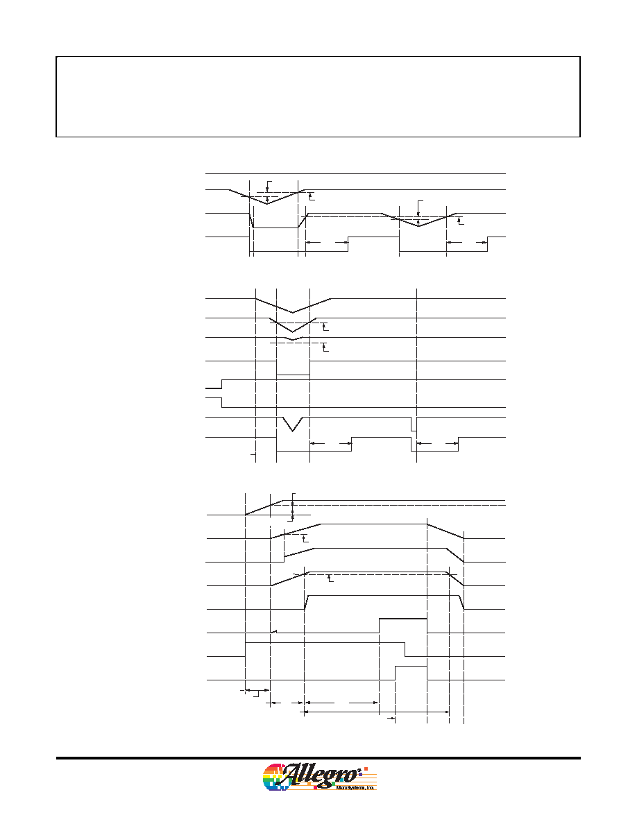
V
REG
V
OUTV33
V
OUTVADJ
V
OUTVADJ
V
ENBAT
V
ENBAT
V
ENB
V
ENB
V
NPOR
V
NPOR
V
NPOR
V
BB
V
REG
V
OUTV33
V
OUTV5A/V5D
VREG Monitor
V
CP
V
REG
V
OUTV33
V
OUTVADJ
V
UVLOV33
t
POR
t
POR
t
POR
t
POR
V
HYSV33
V
UVLOV33
V
BB
> 6 V
V
REG
= 1.8 V
V
UVLOVREG
V
UVLOVADJ
V
HYSVADJ
A B
POR event initiates
+7 V
Slope of V
OUTV33
and V
OUTVADJ
from A to B determined by I
LOAD
and output capacitor (C3, C4).
ENBAT signals power-on
Charge pump ramping
Charge pump OK flag set
V
UVLOV33
exceeded; VADJ enabled
V
UVLO(33)
ENB signals power-off
V33 can sustain regulation with normal load by bulk capacitor (COUT) on V
REG
.
Slope of V
REG
(which controls
V
OUTV5A/V5D
, V
OUTV33
, and V
OUTVADJ
) from A to B determined by I
LOAD
and COUT.
A
B
t
POR
t
SS
Timing Diagrams
Figure 1a. NPOR fault due to undervoltage lockout on the V33 or FB pins
Figure 1b. Power-off using V
BB
Figure 1c. Power-on using ENBAT, followed by power-off using ENB