A1101, A1102, A1103, A1104, and A1106
A1101-DS
Worcester, Massachusetts 01615-0036 (508) 853-5000
115 Northeast Cutoff, Box 15036
www.allegromicro.com
Allegro MicroSystems, Inc.
1
3
2
GND
VOUT
VCC
AB SO LUTE MAX I MUM RAT INGS
Supply Voltage, V
CC
..........................................30 V
Reverse-Supply Voltage, V
RCC
........................ ≠30 V
Output Off Voltage, V
OUT
.................................. 30 V
Reverse-Output Voltage, V
ROUT
..................... ≠0.5 V
Output Current, I
OUTSINK
............................... 25 mA
Magnetic Flux Density, B .........................Unlimited
Operating Temperature
Ambient,
T
A
, Range E.................. ≠40∫C to 85∫C
Ambient,
T
A
, Range L................ ≠40∫C to 150∫C
Maximum
Junction,
T
J(max)
........................165∫C
Storage Temperature, T
S
.................. ≠65∫C to 170∫C
Continuous-time operation
≠ Fast power-on time
≠ Low noise
Stable operation over full operating temperature range
Reverse battery protection
Solid-state reliability
Factory-programmed at end-of-line for optimum performance
Robust EMC performance
High ESD rating
Regulator stability without a bypass capacitor
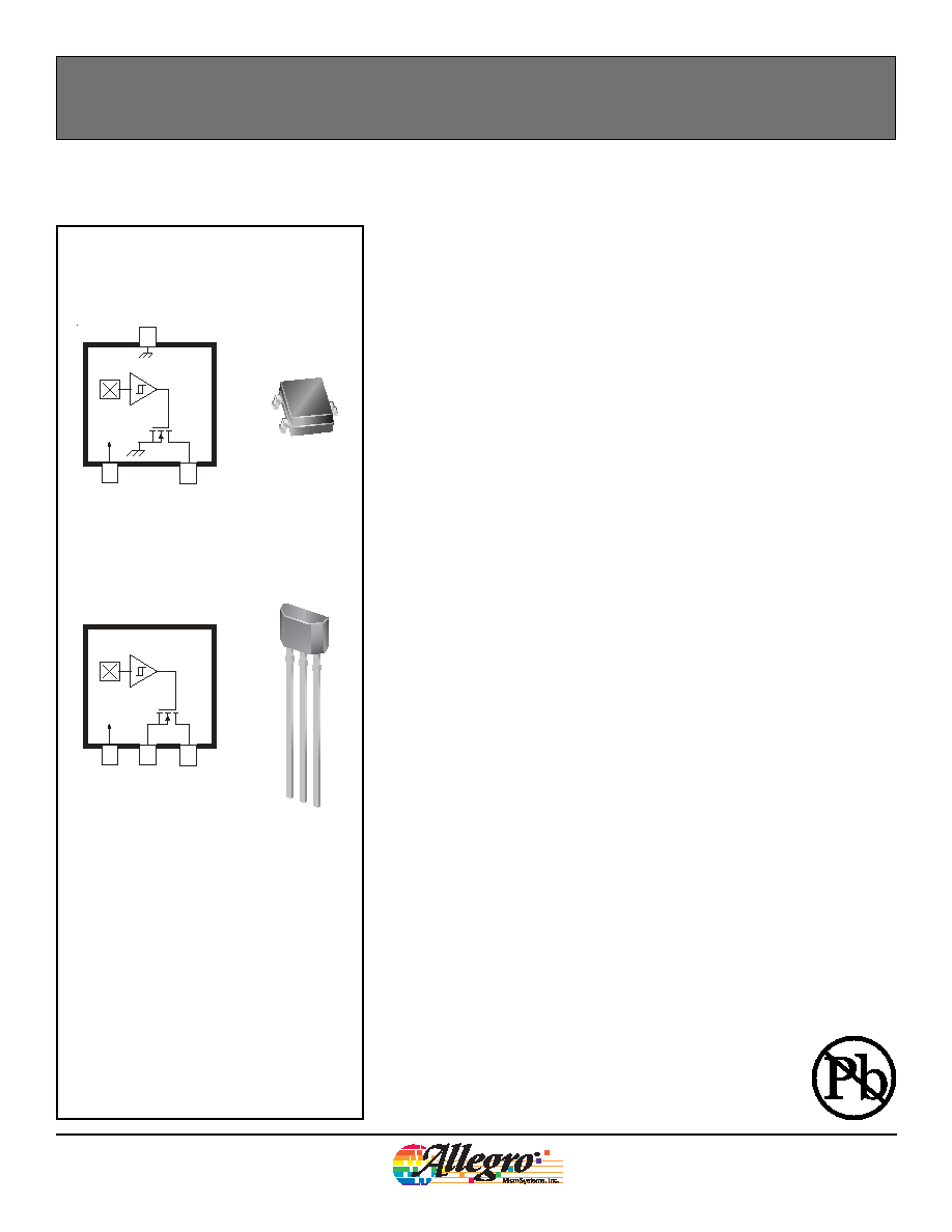
Continuous-Time Switch Family
Features and Benefits
Package UA, 3-pin SIP
Package LH, 3-pin Surface Mount
1
2
3
1
2
3
GND
VOUT
VCC
3
1 2
The Allegro
Æ
A1101-A1104 and A1106 Hall-effect switches are next generation
replacements for the popular Allegro 312x and 314x lines of bipolar switches.
The A110x family, produced with BiCMOS technology, consists of devices that
feature fast power-on time and low-noise operation. Device programming is per-
formed after packaging, to ensure increased switchpoint accuracy by eliminating
offsets that can be induced by package stress. Unique Hall element geometries and
low-offset amplifiers help to minimize noise and to reduce the residual offset volt-
age normally caused by device overmolding, temperature excursions, and thermal
stress.
The A1101-A1104 and A1106 Hall-effect switches include the following on a
single silicon chip: voltage regulator, Hall-voltage generator, small-signal ampli-
fier, Schmitt trigger, and NMOS output transistor. The integrated voltage regulator
permits operation from 3.8 to 24 V. The extensive on-board protection circuitry
makes possible a ±30 V absolute maximum voltage rating for superior protection
in automotive and industrial motor commutation applications, without adding
external components. All devices in the family are identical except for magnetic
switchpoint levels.
The small geometries of the BiCMOS process allow these devices to be pro-
vided in ultrasmall packages. The package styles available provide magnetically
optimized solutions for most applications. Package LH is an SOT23W, a miniature
low-profile surface-mount package, while package UA is a three-lead ultramini
SIP for through-hole mounting. Each package is lead (Pb) free, with 100% matte
tin plated leadframes.
2
A1101-DS
Worcester, Massachusetts 01615-0036 (508) 853-5000
115 Northeast Cutoff, Box 15036
www.allegromicro.com
Allegro MicroSystems, Inc.
Continuous-Time Switch Family
A1101, A1102, A1103, A1104, and A1106
Functional Block Diagram
Amp
Regulator
GND
VCC
VOUT
Offset
Gain
Trim
Control
To all subcircuits
Terminal List
Name
Description
Number
Package LH Package UA
VCC
Connects power supply to chip
1
1
VOUT
Output from circuit
2
3
GND
Ground
3
2
Part Number
Packing*
Mounting
Ambient, T
A
B
RP
(Min)
B
OP
(Max)
A1101ELHLT-T
7-in. reel, 3000 pieces/reel
3-pin SOT23W surface mount
≠40∫C to 85∫C
10
175
A1101EUA-T
Bulk, 500 pieces/bag
3-pin SIP through hole
A1101LLHLT-T
7-in. reel, 3000 pieces/reel
3-pin SOT23W surface mount
≠40∫C to 150∫C
A1101LUA-T
Bulk, 500 pieces/bag
3-pin SIP through hole
A1102ELHLT-T
7-in. reel, 3000 pieces/reel
3-pin SOT23W surface mount
≠40∫C to 85∫C
60
245
A1102EUA-T
Bulk, 500 pieces/bag
3-pin SIP through hole
A1102LLHLT-T
7-in. reel, 3000 pieces/reel
3-pin SOT23W surface mount
≠40∫C to 150∫C
A1102LUA-T
Bulk, 500 pieces/bag
3-pin SIP through hole
A1103ELHLT-T
7-in. reel, 3000 pieces/reel
3-pin SOT23W surface mount
≠40∫C to 85∫C
150
355
A1103EUA-T
Bulk, 500 pieces/bag
3-pin SIP through hole
A1103LLHLT-T
7-in. reel, 3000 pieces/reel
3-pin SOT23W surface mount
≠40∫C to 150∫C
A1103LUA-T
Bulk, 500 pieces/bag
3-pin SIP through hole
A1104ELHLT-T
7-in. reel, 3000 pieces/reel
3-pin SOT23W surface mount
≠40∫C to 85∫C
25
450
A1104EUA-T
Bulk, 500 pieces/bag
3-pin SIP through hole
A1104LLHLT-T
7-in. reel, 3000 pieces/reel
3-pin SOT23W surface mount
≠40∫C to 150∫C
A1104LUA-T
Bulk, 500 pieces/bag
3-pin SIP through hole
A1106ELHLT-T
7-in. reel, 3000 pieces/reel
3-pin SOT23W surface mount
≠40∫C to 85∫C
160
430
A1106EUA-T
Bulk, 500 pieces/bag
3-pin SIP through hole
A1106LLHLT-T
7-in. reel, 3000 pieces/reel
3-pin SOT23W surface mount
≠40∫C to 150∫C
A1106LUA-T
Bulk, 500 pieces/bag
3-pin SIP through hole
*Contact Allegro for additional packing options.
Product Selection Guide
3
A1101-DS
Worcester, Massachusetts 01615-0036 (508) 853-5000
115 Northeast Cutoff, Box 15036
www.allegromicro.com
Allegro MicroSystems, Inc.
Continuous-Time Switch Family
A1101, A1102, A1103, A1104, and A1106
ELECTRICAL OPERATING CHARACTERISTICS over full operating voltage and ambient temperature ranges, unless otherwise noted
Characteristic
Symbol
Test Conditions
Min.
Typ.
Max.
Units
Supply Voltage
1
V
CC
Operating, T
J
< 165∞C
3.8
≠
24
V
Output Leakage Current
I
OUTOFF
V
OUT
= 24 V, B < B
RP
≠
≠
10
µA
Output On Voltage
V
OUT(SAT)
I
OUT
= 20 mA, B > B
OP
≠
215
400
mV
Power-On Time
2
t
PO
Slew rate (dV
CC
/dt) < 2.5 V/µs, B > B
OP
+ 5 G or
B < B
RP
≠ 5 G
≠
≠
4
µs
Output Rise Time
3
t
r
V
CC
= 12 V, R
LOAD
= 820 , C
S
= 12 pF
≠
≠
400
ns
Output Fall Time
3
t
f
V
CC
= 12 V, R
LOAD
= 820 , C
S
= 12 pF
≠
≠
400
ns
Supply Current
I
CCON
B > B
OP
≠
4.1
7.5
mA
I
CCOFF
B < B
RP
≠
3.8
7.5
mA
Reverse Battery Current
I
RCC
V
RCC
= ≠30 V
≠
≠
≠10
mA
Supply Zener Clamp Voltage
V
Z
I
CC
= 10.5 mA; T
A
= 25∞C
32
≠
≠
V
Supply Zener Current
4
I
Z
V
Z
= 32 V; T
A
= 25∞C
≠
≠
10.5
mA
1
Maximum voltage must be adjusted for power dissipation and junction temperature, see Power Derating section.
2
For V
CC
slew rates greater than 250 V/µs, and T
A
= 150∞C, the Power-On Time can reach its maximum value.
3
C
S
=oscilloscope probe capacitance.
4
Maximum current limit is equal to the maximum I
CC(max)
+ 3 mA.
DEVICE QUALIFICATION PROGRAM
Contact Allegro for information.
EMC (Electromagnetic Compatibility) REQUIREMENTS
Contact Allegro for information.
4
A1101-DS
Worcester, Massachusetts 01615-0036 (508) 853-5000
115 Northeast Cutoff, Box 15036
www.allegromicro.com
Allegro MicroSystems, Inc.
Continuous-Time Switch Family
A1101, A1102, A1103, A1104, and A1106
MAGNETIC OPERATING CHARACTERISTICS
1
over full operating voltage and ambient temperature ranges, unless otherwise noted
Characteristic
Symbol
Test Conditions
Min.
Typ.
Max.
Units
Operate Point
B
OP
A1101
T
A
= 25∞C
50
100
160
G
Operating Temperature Range
30
100
175
G
A1102
T
A
= 25∞C
130
180
230
G
Operating Temperature Range
115
180
245
G
A1103
T
A
= 25∞C
220
280
340
G
Operating Temperature Range
205
280
355
G
A1104
T
A
= 25∞C
70
≠
350
G
Operating Temperature Range
35
≠
450
G
A1106
T
A
= 25∞C
280
340
400
G
Operating Temperature Range
260
340
430
G
Release Point
B
RP
A1101
T
A
= 25∞C
10
45
130
G
Operating Temperature Range
10
45
145
G
A1102
T
A
= 25∞C
75
125
175
G
Operating Temperature Range
60
125
190
G
A1103
T
A
= 25∞C
165
225
285
G
Operating
Temperature
Range
150 225 300 G
A1104
T
A
= 25∞C
50
≠
330
G
Operating Temperature Range
25
≠
430
G
A1106
T
A
= 25∞C
180
240
300
G
Operating Temperature Range
160
240
330
G
Hysteresis
B
HYS
A1101
T
A
= 25∞C
20
55
80
G
Operating Temperature Range
20
55
80
G
A1102
T
A
= 25∞C
30
55
80
G
Operating Temperature Range
30
55
80
G
A1103
T
A
= 25∞C
30
55
80
G
Operating Temperature Range
30
55
80
G
A1104
T
A
= 25∞C
20
55
≠
G
Operating Temperature Range
20
55
≠
G
A1106
T
A
= 25∞C
70
105
140
G
Operating Temperature Range
70
105
140
G
1
Magnetic flux density, B, is indicated as a negative value for north-polarity magnetic fields, and as a positive value for south-polarity magnetic fields.
This so-called algebraic convention supports arithmetic comparison of north and south polarity values, where the relative strength of the field is indicated
by the absolute value of B, and the sign indicates the polarity of the field (for example, a ≠100 G field and a 100 G field have equivalent strength, but
opposite polarity).
5
A1101-DS
Worcester, Massachusetts 01615-0036 (508) 853-5000
115 Northeast Cutoff, Box 15036
www.allegromicro.com
Allegro MicroSystems, Inc.
Continuous-Time Switch Family
A1101, A1102, A1103, A1104, and A1106
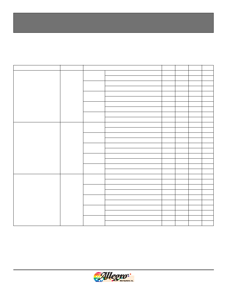
THERMAL CHARACTERISTICS may require derating at maximum conditions, see application information
Characteristic
Symbol
Test Conditions
Value Units
Package Thermal Resistance
R
JA
Package LH, minimum-K PCB (single layer, single-sided with
copper limited to solder pads)
110
∫C/W
Package LH, low-K PCB (single layer, double-sided with
0.926 in
2
copper area)
228
∫C/W
Package UA, minimum-K PCB (single layer, single-sided with
copper limited to solder pads)
165
∫C/W
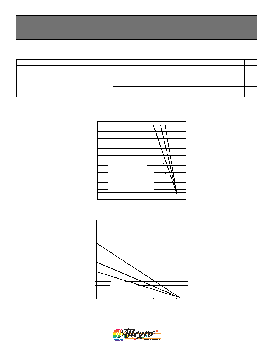
6
7
8
9
2
3
4
5
10
11
12
13
14
15
16
17
18
19
20
21
22
23
24
25
20
40
60
80
100
120
140
160
180
Maximum
Allowable
V
CC
(V)
T
J(max)
= 165∫C; I
CC
= I
CC(max)
Power Derating Curve
(R
JA
= 228 ∫C/W)
Minimum-K PCB, Package LH
(R
JA
= 110 ∫C/W)
Low-K PCB, Package LH
(R
JA
= 165 ∫C/W)
Minimum-K PCB, Package UA
V
CC(min)
V
CC(max)
0
100
200
300
400
500
600
700
800
900
1000
1100
1200
1300
1400
1500
1600
1700
1800
1900
20
40
60
80
100
120
140
160
180
Temperature (∞C)
P
o
w
e
r
D
i
s
s
i
pa
ti
on
,
P
D
(m
W)
Power Dissipation versus Ambient Temperature
(R
JA
= 165
∫C/W)
Minimum-K
PCB,
Pac
kag
e UA
(R
JA
= 228 ∫C/
W)
Minimu
m-K PCB,
Packa
ge LH
(R
JA
= 110
∫C/W)
Low-K
PCB,
Package
LH