 | –≠–ª–µ–∫—Ç—Ä–æ–Ω–Ω—ã–π –∫–æ–º–ø–æ–Ω–µ–Ω—Ç: A1425 | –°–∫–∞—á–∞—Ç—å:  PDF PDF  ZIP ZIP |

A1425
A1425-DS Rev. 0b
Worcester, Massachusetts 01615-0036 (508) 853-5000
115 Northeast Cutoff, Box 15036
www.allegromicro.com
Allegro MicroSystems, Inc.
AB SO LUTE MAX I MUM RAT INGS
Supply Voltage, V
CC
..........................................28 V
Reverse-Supply Voltage, V
RCC
........................ ≠18 V
Output Current, I
OUT
.......................................25 mA
Reverse-Output Current, I
ROUT
.....................≠50 mA
Reverse-Output Voltage, V
ROUT
...................≠50 mA
Operating Temperature
Ambient,
T
A
................................ ≠40∫C to 150∫C
Maximum
Junction,
T
J(max)
........................165∫C
Storage Temperature, T
S
.................. ≠65∫C to 170∫C
Use the following complete part number when ordering:
Package K, 4-pin SIP
Features and Benefi ts
The A1425 ac-coupled Hall-effect sensor is a monolithic integrated circuit that
switches in response to changing differential magnetic fi elds created by rotating
ring magnets or, when coupled with a magnet, by ferrous targets. The device is a
true zero-crossing detector: the output switches precisely when the difference in
magnetic fi eld strength between the two Hall elements is zero. A unique dual-
comparator scheme provides for accurate switching during zero-crossing, both
when the sensed fi eld is increasing in strength and when it is decreasing, while
utilizing hysteresis to prevent false switching. The zero-crossing nature of this
device provides excellent repeatability for crankshaft applications.
Changes in fi eld strength at the device face caused by a moving target are sensed
by the two integrated Hall transducers, generating signals that are differen-
tially amplifi ed by on-chip electronics. This differential sensing design provides
immunity to radial vibration within the operating air gap range of the A1425, by
rejection of the common mode signal. Steady-state magnet and system offsets are
eliminated using an on-chip differential band-pass fi lter. This fi lter also provides
relative immunity to interference from electromagnetic sources.
The device utilizes advanced temperature compensation for the high-pass fi lter,
sensitivity, and the Schmitt trigger switchpoints, guaranteeing optimal operation to
low frequencies over a wide range of air gaps and temperatures.
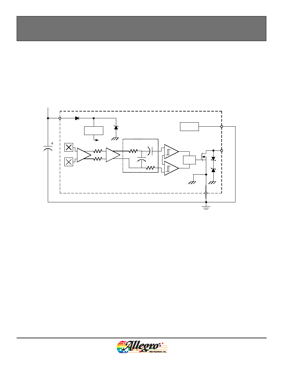
Each Hall effect digital integrated circuit includes a voltage regulator, two Hall
effect sensing elements, temperature compensating circuitry, a low-level ampli-
fi er, band-pass fi lter, Schmitt trigger, and an output driver. The on-board regulator
permits operation with supply voltages from 4.0 to 26.5 V. The output stage can
easily switch 20 mA over the full frequency response range of the sensor, and is
compatible with both TTL and CMOS logic circuits.
The device is packaged in a 4-pin plastic SIP (part number suffi x -K).
∑ Senses motion of ring magnet targets
∑ Integrated fi lter capacitor
∑ Wide operating temperature range
∑ Operation with frequency of sensed transitions from 20 Hz to 30 kHz
∑ EMI-resistant
∑ Large working air gaps
∑ 4.0 to 26.5 V operating range
∑ Output compatible with both TTL and CMOS logic families
∑ Reverse battery protection
Part Number
Package
Ambient (∫C)
A1425LK
4-pin plastic SIP
≠40 to 150
1. VCC
2. VOUT
3. Test pin, tie to GND
4. GND
1
2
3
4
High Accuracy Analog Speed Sensor with Integrated Filter Capacitor
and Dual Zero-Crossing Output Signal
Preliminary Data Sheet
Subject to Change Without Notice
November 10, 2004
Engineering samples available on a limited basis. Contact your local
sales or applications support offi ce for additional information.
2
A1425-DS Rev. 0b
Worcester, Massachusetts 01615-0036 (508) 853-5000
115 Northeast Cutoff, Box 15036
www.allegromicro.com
Allegro MicroSystems, Inc.
High Accuracy Analog Speed Sensor with Integrated Filter Capacitor and Dual Zero-Crossing Output Signal
A1425
Functional Block Diagram
Hall
Amp
Regulator
Bandpass Filter Integrated
Tracking Capacitor
VOUT
(Pin 2)
VCC
(Pin 1)
GND
(Pin 4)
0.1 uF
V+
Diagnostic
Circuitry
Gain
Stage
Dual Hall
Elements
Dual
Comparators
Logic
Test Pin
(Pin 3)
Preliminary - Subject to Change
Without Notice November 10, 2004
3
A1425-DS Rev. 0b
Worcester, Massachusetts 01615-0036 (508) 853-5000
115 Northeast Cutoff, Box 15036
www.allegromicro.com
Allegro MicroSystems, Inc.
High Accuracy Analog Speed Sensor with Integrated Filter Capacitor and Dual Zero-Crossing Output Signal
A1425
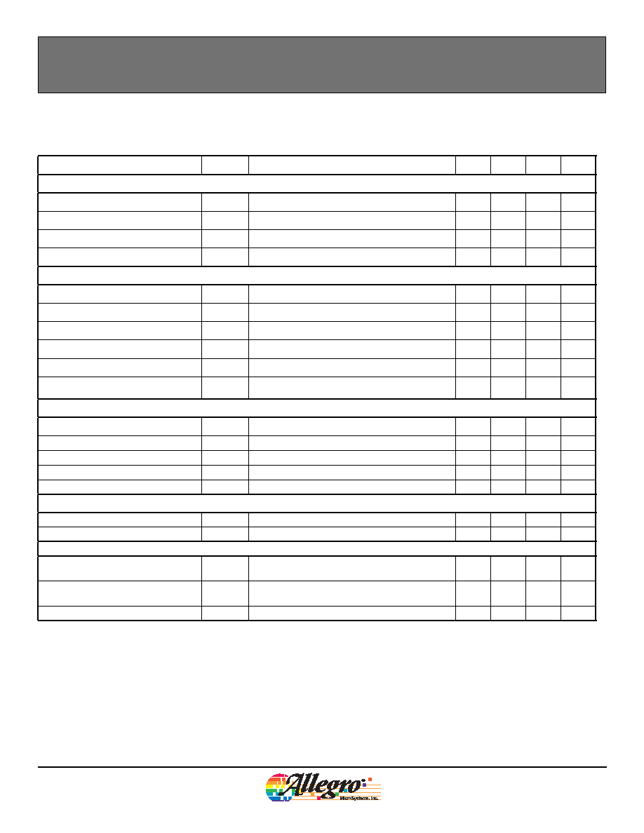
OPERATING CHARACTERISTICS
Valid at T
A
= ≠ 40
∫
C to 150
∫
C, T
J
165∞C; over operational air gap range and V
CC
within
operating range, unless otherwise noted. Typical operating parameters: V
CC
= 12 V and T
A
= 25∞C.
Characteristic
Symbol
Test Conditions
Min.
Typ.
Max.
Units
ELECTRICAL CHARACTERISTICS
Supply Voltage
V
CC
Operating; T
J
< T
J(max)
4.0
≠
26.5
V
Supply Current
I
CC
≠
4.2
7.0
mA
Output Saturation Voltage
V
OUT(SAT)
I
SINK
= 20 mA
≠
140
400
mV
Output Leakage Current
I
OFF
V
OUT
= 24 V, B
diff
= 0
≠
≠
5
µA
PROTECTION COMPONENT CHARACTERISTICS
Reverse Supply Current
I
RCC
V
CC
= ≠18 V
≠
≠
≠1
mA
Supply Zener Current
I
ZCC
V
CC
= 28 V
≠
≠
10
mA
Supply Zener Clamp Voltage
V
ZCC
I
CC
= 10 mA
1
, T
A
= 25∞C
28
33
37
V
Output Zener Current
I
ZOUT
V
OUT
= 28 V
≠
≠
3
mA
Output Zener Clamp Voltage
V
ZOUT
I
OUT
= 3 mA, T
A
= 25∞C
28
≠
≠
V
Output Short Circuit Current Limit
I
OUT(lim)
≠
≠
50
mA
RESPONSE CHARACTERISTICS
Power-On Time
2,6
t
PO
V
CC
> V
CC(min)
≠
4.5
9
ms
Settling Time
3,6
t
S
f
Bdiff
100 Hz
0
≠
50
ms
Response Time
6
t
R
Equal to t
PO
+ t
S
;
f
Bdiff
100 Hz
4.5
≠
59
ms
Upper Corner Frequency
f
cu
≠3 dB, single pole
30
≠
≠
kHz
Lower Corner Frequency
f
cl
≠3 dB, single pole
≠
≠
20
Hz
OUTPUT CHARACTERISTICS
Output Rise Time
4
t
r
R
PU
= 1 k, C = 10 pF
≠
≠
200
ns
Output Fall Time
t
f
R
PU
= 1 k, I
SINK
= 20 mA, C = 10 pF
≠
≠
200
ns
MAGNETIC CHARACTERISTICS
Output Off Switchpoint
5,6
B
OP
B
diff
increasing, f
Bdiff
= 200 Hz, B
diff
= 50 Gp-p;
digital output signal switches low to high
≠11
0
11
G
Output On Switchpoint
5,6
B
RP
B
diff
decreasing, f
Bdiff
= 200 Hz, B
diff
= 50 Gp-p;
digital output signal switches high to low
≠11
0
11
G
Applied Magnetic Field
6,7
B
diff
Differential p-p magnetic fi eld
50
≠
1250
G
1
Equivalent to I
CC(max)
+ 3 mA.
2
Time required to initialize device.
3
Time required for the output switchpoints to be within specifi cation.
4
Output Rise Time will be dominated by the RC time constant.
5
For other sinusoidal signal frequencies and magnetic fi elds, ≠B
OP
= B
RP
= sin(B
diff
/ 2) ± 25%, where is the phase shift shown in the Characteristic
Data section.
6
See Defi nitions of Terms section.
7
Exceeding the maximum magnetic fi eld may result in compromised absolute accuracy.
Preliminary - Subject to Change
Without Notice November 10, 2004

4
A1425-DS Rev. 0b
Worcester, Massachusetts 01615-0036 (508) 853-5000
115 Northeast Cutoff, Box 15036
www.allegromicro.com
Allegro MicroSystems, Inc.
High Accuracy Analog Speed Sensor with Integrated Filter Capacitor and Dual Zero-Crossing Output Signal
A1425
THERMAL CHARACTERISTICS
may require derating at maximum conditions, see application information
Characteristic
Symbol
Test Conditions
Min. Typ.
Max Units
Package Thermal Resistance
R
JA
Minimum-K PCB (single-sided with copper limited to
solder pads)
177
≠
≠
∫C/W
20
40
60
80
100
120
140
160
180
Maximum
Allowable
V
CC
(V)
T
J(max)
= 165∫C; I
CC
= I
CC(max)
Power Derating Curve
8
10
12
14
0
2
4
6
16
18
20
22
24
26
28
30
(R
JA
= 177 ∫C/W)
Minimum-K PCB
V
CC(min)
V
CC(max)
20
40
60
80
100
120
140
160
180
Temperature (∞C)
P
o
w
e
r
D
i
s
s
i
pa
ti
on
,
P
D
(m
W)
T
J(max)
= 165∫C; V
CC
= V
CC(max)
; I
CC
= I
CC(max)
Maximum Power Dissipation, P
D(max)
(R
JA
= 1
77
∫C/W)
Minimum-K
PCB
0
50
100
150
200
250
300
350
400
450
500
550
600
650
700
750
800
850
900
The following provide additional information about some of
the parameters cited in the Operating Characteristics table.
For additional information, visit the Allegro Web site at
www.allegromicro.com.
Applied Magnetic Field, B
diff
≠ The differential magnetic fl ux
density which is calculated as the arithmetic difference of the
fl ux densities observed by each of the two Hall elements.
Output Off Switchpoint (Operate Point), B
OP
≠ The value of
increasing differential magnetic fl ux density at which the device
output switches from low to high. This value may be greater than
or less than 0 G.
Output On Switchpoint (Release Point), B
RP
≠ The value of
decreasing differential magnetic fl ux density at which the device
output switches from high to low. This value may be greater
than or less than 0 G.
Power-On Time, t
PO
≠ The time needed by the device, after
power is applied, to initialize all circuitry necessary for proper
operation.
Settling Time, t
S
≠ The time required by the device, after t
PO
,
and after a valid magnetic signal has been applied, to provide
proper output transitions. Settling time is a function of magnetic
offset, offset polarity, signal phase, signal frequency, and signal
amplitude.
Response Time ≠ The total time required for generating zero-
crossing output transitions after power-up (the sum of power-on
time and settling time).
Defi nitions of Terms
Preliminary - Subject to Change
Without Notice November 10, 2004

5
A1425-DS Rev. 0b
Worcester, Massachusetts 01615-0036 (508) 853-5000
115 Northeast Cutoff, Box 15036
www.allegromicro.com
Allegro MicroSystems, Inc.
High Accuracy Analog Speed Sensor with Integrated Filter Capacitor and Dual Zero-Crossing Output Signal
A1425
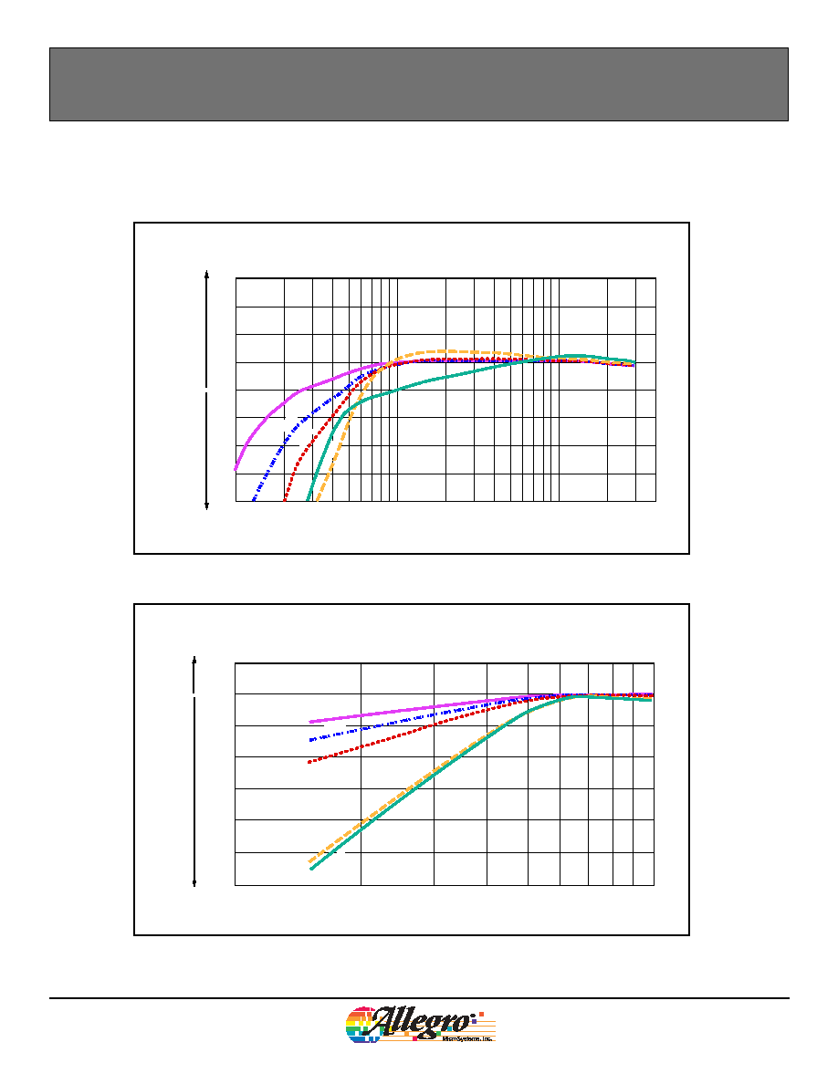
Empirical Results
4.5
20.0
12.0
V
CC
(V)
4.5
20.0
12.0
V
CC
(V)
4.5
20.0
12.0
V
CC
(V)
150
≠40
25
T
A
(∫C)
150
≠40
25
T
A
(∫C)
150
≠40
25
T
A
(∫C)
I
CC(OFF)
by T
A
Ambient Temperature, T
A
(∫C)
Current
(mA)
10.0
9.0
8.0
7.0
6.0
5.0
4.0
3.0
2.0
1.0
0.0
≠50
0
50
100
150
200
Over V
CC
Range
I
CC(OFF)
by V
CC
Supply Voltage, V
CC
(V)
Current
(mA)
10.0
9.0
8.0
7.0
6.0
5.0
4.0
3.0
2.0
1.0
0.0
0
5
10
15
20
25
Over T
A
Range
I
CC(ON)
by V
CC
Supply Voltage, V
CC
(V)
Current
(mA)
10.0
9.0
8.0
7.0
6.0
5.0
4.0
3.0
2.0
1.0
0.0
0
5
10
15
20
25
Over T
A
Range
Supply Voltage, V
CC
(V)
0
5
10
15
20
25
I
CC(ON)
by T
A
Ambient Temperature, T
A
(∫C)
Current
(mA)
10.0
9.0
8.0
7.0
6.0
5.0
4.0
3.0
2.0
1.0
0.0
≠50
0
50
100
150
200
Over V
CC
Range
V
OUT(SAT)
by T
A
Ambient Temperature, T
A
(∫C)
V
oltage
(mV)
500
450
400
350
300
250
200
150
100
50
0
≠50
0
50
100
150
200
Over V
CC
Range; I
SINK
= 20 mA
V
OUT(SAT)
by V
CC
V
oltage
(mV)
500
450
400
350
300
250
200
150
100
50
0
Over T
A
Range; I
SINK
= 20 mA
Continued on next page.
Preliminary - Subject to Change
Without Notice November 10, 2004

6
A1425-DS Rev. 0b
Worcester, Massachusetts 01615-0036 (508) 853-5000
115 Northeast Cutoff, Box 15036
www.allegromicro.com
Allegro MicroSystems, Inc.
High Accuracy Analog Speed Sensor with Integrated Filter Capacitor and Dual Zero-Crossing Output Signal
A1425
Empirical Results, continued
Air Gap (mm)
Repeatability
(
∫
o
f
Rotation)
Air Gap (mm)
Repeatability
(
∫
o
f
Rotation)
Preliminary - Subject to Change
Without Notice November 10, 2004

7
A1425-DS Rev. 0b
Worcester, Massachusetts 01615-0036 (508) 853-5000
115 Northeast Cutoff, Box 15036
www.allegromicro.com
Allegro MicroSystems, Inc.
High Accuracy Analog Speed Sensor with Integrated Filter Capacitor and Dual Zero-Crossing Output Signal
A1425
Simulation Results
Typical Applied Magnetic Fields, B
diff
by Frequency of Sensed Transitions
Over the Range of Ambient Operating Temperatures, T
A
B
dif
f(min)
(G)
Frequency, f
Bdiff
(kHz)
0.01
0.1
1
10
13
40
0
35
5
30
10
25
15
20
150
25
≠40
Typical Phase Shifts, by Frequency of Sensed Transitions
Over the Range of Applied Magnetic Fields, B
diff
(G
P-P
)
Phase
Shift
(∫)
Frequency, f
Bdiff
(kHz)
0.01
0.1
1
10
13
40
0
30
≠30
20
≠50
≠60
≠40
≠20
10
≠10
50
100
500
1250
750
Continued on next page.
Preliminary - Subject to Change
Without Notice November 10, 2004
8
A1425-DS Rev. 0b
Worcester, Massachusetts 01615-0036 (508) 853-5000
115 Northeast Cutoff, Box 15036
www.allegromicro.com
Allegro MicroSystems, Inc.
High Accuracy Analog Speed Sensor with Integrated Filter Capacitor and Dual Zero-Crossing Output Signal
A1425
Simulation Results, continued
50
100
500
750
1250
Typical Output Signal Delay by Frequency of Sensed Transitions, >100 Hz
Over the Range of Applied Magnetic Fields, B
diff
(G
P-P
)
I
OUT
Delay
(
µ
s)
I
OUT
Lagging
I
OUT
Leading
Frequency, f
Bdiff
(kHz)
0.1
1
10
13
20
≠20
15
≠15
10
≠10
5
≠5
0
50
100
500
750
1250
Typical Output Signal Delay by Frequency of Sensed Transitions, 0 to 100 Hz
Over the Range of Applied Magnetic Fields, B
diff
(G
P-P
)
I
OUT
Delay
(
µ
s)
I
OUT
Lagging
I
OUT
Leading
Frequency, f
Bdiff
(Hz)
0
100
1000
0
≠1000
≠2000
≠3000
≠4000
≠5000
≠6000
Preliminary - Subject to Change
Without Notice November 10, 2004

9
A1425-DS Rev. 0b
Worcester, Massachusetts 01615-0036 (508) 853-5000
115 Northeast Cutoff, Box 15036
www.allegromicro.com
Allegro MicroSystems, Inc.
High Accuracy Analog Speed Sensor with Integrated Filter Capacitor and Dual Zero-Crossing Output Signal
A1425
Sensor Evaluation: EMC Characterization
Test Name
Reference Specifi cation
ESD ≠ Human Body Model
*
AEC-Q100-002
ESD ≠ Machine Model
AEC-Q100-003
Conducted Transients
ISO 7637-1
Direct RF Injection
ISO 11452-7
Bulk Current Injection
ISO 11452-4
TEM Cell
ISO 11452-3
*
ESD test is done with no external components.
Please contact Allegro MicroSystems for EMC performance information.
(EMC test results are available after review of fi rst silicon.)
1425
Vs
C1
R2
1
VCC
3
Test
VOUT
GND
2
4
R1
C2
Component
Value
Units
R1
*
1.2
k
R2
100
C1
0.1
µF
C2
0.1
F
*
Pull-up resistor not required for
protection but for normal operation.
Recommended EMC test circuit. Test circuit recommended
confi guration may change after evaluation of fi rst silicon.
Preliminary - Subject to Change
Without Notice November 10, 2004
10
A1425-DS Rev. 0b
Worcester, Massachusetts 01615-0036 (508) 853-5000
115 Northeast Cutoff, Box 15036
www.allegromicro.com
Allegro MicroSystems, Inc.
High Accuracy Analog Speed Sensor with Integrated Filter Capacitor and Dual Zero-Crossing Output Signal
A1425
Applications Information
The A1425 is a versatile high-precision differential sensing
device that can be used in a wide range of applications. Proper
choice of the target material and shape, and assembly techniques
enables large working air gaps and high switchpoint accuracy
over the device operating temperature range.
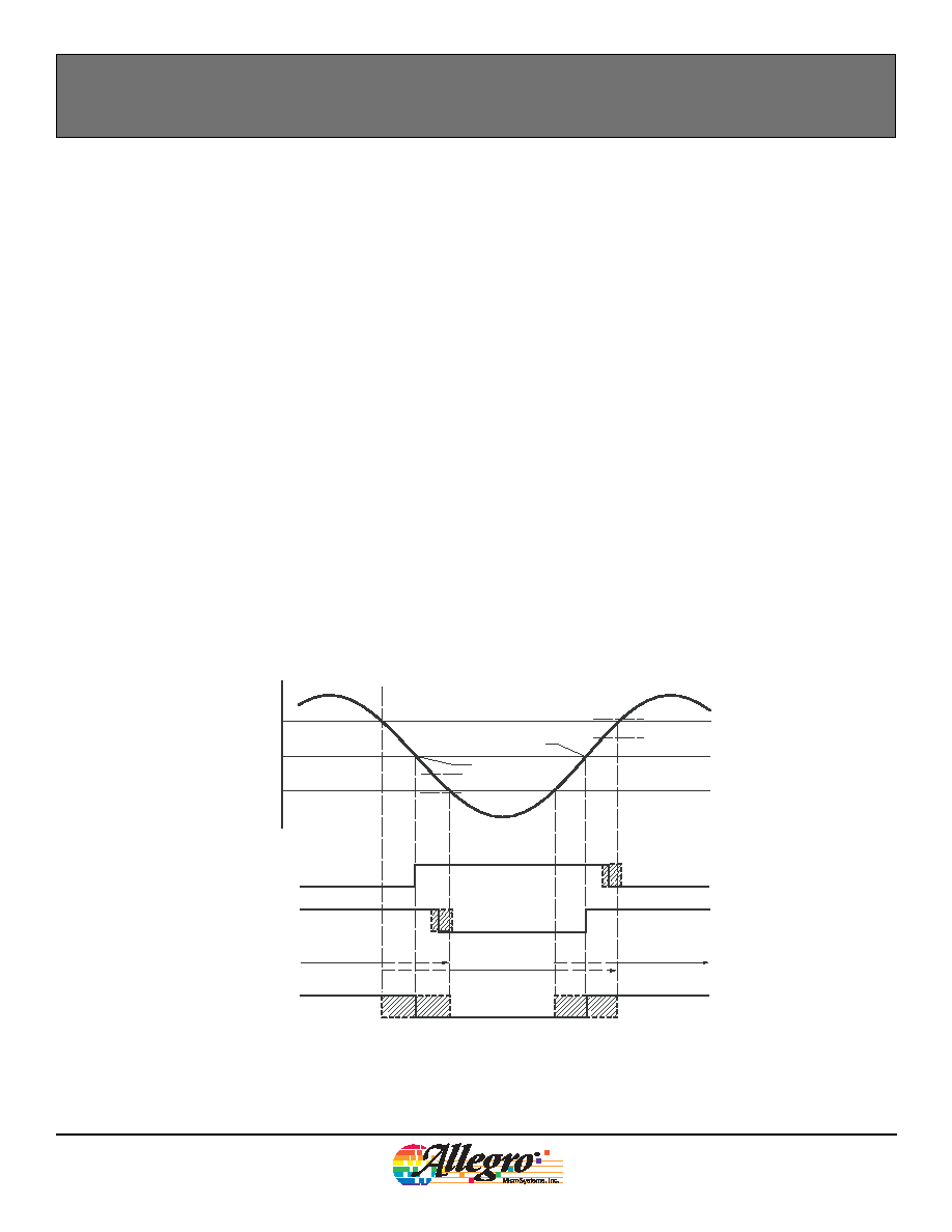
Sensor Operation
The A1425 sensor IC contains two integrated Hall transducers
that are used to differentially sense a magnetic fi eld across the
surface of the IC. Referring to fi gure 1, the trigger switches the
output off (output high) when the differential magnetic fi eld
crosses zero while increasing in strength (referred to a the posi-
tive direction), and switches the output on (output low) when
the differential magnetic fi eld crosses zero while decreasing (the
negative direction).
The operation is achieved through the use of two separate com-
parators. Both comparators use the same reference point, 0 G, to
provide high accuracy, but one comparator has a positive hystere-
sis, B
HYS1
, and the other a negative hysteresis, B
HYS2
. Therefore,
one comparator switches at the zero crossing on an increasing
differential signal and the other switches at the zero crossing on a
decreasing differential signal. The hysteresis on each comparator
precludes false switching on noise or target jitter.
Start-up
During power-on time, t
PO
, the output signal, V
OUT
, is high.
Beyond this time, if the applied magnetic fi eld, B
diff
, is absent or
less than 50 G peak-to-peak, the switching state and V
OUT
polar-
ity are indeterminate. V
OUT
will be valid for B
diff
> 50 Gp-p,
after the additional settling time, t
S
, has also elapsed.
Also during t
PO
, a circuit in the A1425 is briefl y enabled that
charges the on-chip capacitor. This feature reduces t
PO
, relative
to the long RC time constant of a high-pass fi lter.
Delay
The on-chip band-pass fi lter induces delay in the output signal,
V
OUT
, relative to the applied magnetic fi eld, B
diff
. Simulation
data shown in the Characteristic Data section quantify the effect
of the input signal amplitude on the phase shift of the output.
Figure 1. Typical output characteristics with dual comparator operation. Characteristics shown without delay, see characteristic
data charts for delay and phase shift contributions.
11.0
0.0
≠11.0
On
Off
Off
B
RP(typ)
B
OP(typ)
B
OP(min)
/ B
RP(min)
B
OP(max)
/ B
RP(max)
Output Signal, V
OUT
Switching State
Applied Magnetic
Field, B
diff
Comparator 1
Comparator 2
t+
B
HYS2
A
B
HYS1
A
Preliminary - Subject to Change
Without Notice November 10, 2004
11
A1425-DS Rev. 0b
Worcester, Massachusetts 01615-0036 (508) 853-5000
115 Northeast Cutoff, Box 15036
www.allegromicro.com
Allegro MicroSystems, Inc.
High Accuracy Analog Speed Sensor with Integrated Filter Capacitor and Dual Zero-Crossing Output Signal
A1425
2
A1425
1
3
4
VOUT
0.1 uF
R
PU
VCC
AC-Coupled Operation
Steady-state magnet and system offsets are eliminated using an
on-chip differential band-pass fi lter. The low and high frequency
poles of this band-pass fi lter are set using internal integrated
capacitors and resistors. The differential structure of this fi lter
improves the ability of the IC to reject single-ended noise on
the ground (GND pin) or supply line (VCC pin) and, as a result,
makes it more resistant to electromagnetic interference typically
seen in hostile remote-sensing environments.
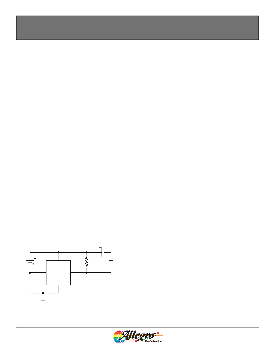
Power Supply Protection
The A1425 contains an on-chip voltage regulator and can oper-
ate over a wide supply voltage range. In applications that operate
the device from an unregulated power supply, transient protec-
tion must be added externally. For applications using a regulated
line, EMI/RFI protection may still be required. The circuit
shown in fi gure 2 is the most basic confi guration required for
proper device operation.
Figure 2. Basic application circuit
. A pull-up resistor is required with
the output driver.
Power Derating
The device must be operated below the maximum junction
temperature of the device, T
J(max)
. Under certain combinations of
peak conditions, reliable operation may require derating sup-
plied power or improving the heat dissipation properties of the
application. This section presents a procedure for correlating
factors affecting operating T
J
. (Thermal data is also available on
the Allegro MicroSystems Web site.)
The Package Thermal Resistance, R
JA
, is a fi gure of merit sum-
marizing the ability of the application and the device to dissipate
heat from the junction (die), through all paths to the ambient air.
Its primary component is the Effective Thermal Conductivity,
K, of the printed circuit board, including adjacent devices and
traces. Radiation from the die through the device case, R
JC
, is
relatively small component of R
JA
. Ambient air temperature,
T
A
, and air motion are signifi cant external factors, damped by
overmolding.
The effect of varying power levels (Power Dissipation, P
D
), can
be estimated. The following formulas represent the fundamental
relationships used to estimate T
J
, at P
D
.
P
D
= V
IN
◊
I
IN
(1)
T = P
D
◊
R
JA
(2)
T
J
= T
A
+ T
(3)
For example, given common conditions such as: T
A
= 25∞C,
V
CC
= 12 V, I
CC
= 4.2 mA, and R
JA
= 177 ∞C/W, then:
P
D
= V
CC
◊
I
CC
= 12 V
◊
4.2 mA = 50 mW
T = P
D
◊
R
JA
= 50 mW
◊
177 ∞C/W = 9∞C
T
J
= T
A
+
T = 25∞C + 9∞C = 34∞C
A worst-case estimate, P
D(max)
, represents the maximum allow-
able power level (V
CC(max)
, I
CC(max)
), without exceeding T
J(max)
,
at a selected R
JA
and T
A
.
Example
Reliability for V
CC
at T
A
=
150∞C, package L-I1, using minimum-
K PCB
Observe the worst-case ratings for the device, specifi cally:
R
JA
=
177∞C/W, T
J(max)
=
165∞C, V
CC(max)
=
26.5
V, and
I
CC(max)
=
7.0
mA.
Calculate the maximum allowable power level, P
D(max)
. First,
invert equation 3:
T
max
= T
J(max)
≠ T
A
= 165
∞C
≠
150
∞C = 15
∞C
This provides the allowable increase to T
J
resulting from internal
power dissipation. Then, invert equation 2:
P
D(max)
=
T
max
˜ R
JA
= 15∞C ˜ 177 ∞C/W = 91 mW
Finally, invert equation 1 with respect to voltage:
V
CC(est)
= P
D(max)
˜ I
CC(max)
= 91 mW ˜ 7.0 mA = 13 V
The result indicates that, at T
A
, the application and device can
dissipate adequate amounts of heat at voltages V
CC(est)
.
Compare V
CC(est)
to V
CC(max)
. If V
CC(est)
V
CC(max)
, then reli-
able operation between V
CC(est)
and V
CC(max)
requires enhanced
R
JA
. If V
CC(est)
V
CC(max)
, then operation between V
CC(est)
and
V
CC(max)
is reliable under these conditions.
Preliminary - Subject to Change
Without Notice November 10, 2004

12
A1425-DS Rev. 0b
Worcester, Massachusetts 01615-0036 (508) 853-5000
115 Northeast Cutoff, Box 15036
www.allegromicro.com
Allegro MicroSystems, Inc.
High Accuracy Analog Speed Sensor with Integrated Filter Capacitor and Dual Zero-Crossing Output Signal
A1425
Package K, 4-pin SIP
The products described herein are manufactured under one or
more of the following U.S. patents: 5,045,920; 5,264,783; 5,442,283;
5,389,889; 5,581,179; 5,517,112; 5,619,137; 5,621,319; 5,650,719;
5,686,894; 5,694,038; 5,729,130; 5,917,320; and other patents pend-
ing.
Allegro MicroSystems, Inc. reserves the right to make, from time to
time, such de par tures from the detail spec i fi ca tions as may be required
to permit improvements in the per for mance, reliability, or manufactur-
ability of its products. Before placing an order, the user is cautioned to
verify that the information being relied upon is current.
Allegro products are not authorized for use as critical components in
life-support devices or sys tems without express written approval.
The in for ma tion in clud ed herein is believed to be ac cu rate and reli-
able. How ev er, Allegro MicroSystems, Inc. assumes no re spon si bil i ty
for its use; nor for any in fringe ment of patents or other rights of third
parties which may result from its use.
Copyright © 2004 Allegro MicroSystems, Inc.
Preliminary - Subject to Change
Without Notice November 10, 2004