A1441
A1441-DS
Worcester, Massachusetts 01615-0036 (508) 853-5000
115 Northeast Cutoff, Box 15036
www.allegromicro.com
Allegro MicroSystems, Inc.
AB SO LUTE MAX I MUM RAT INGS
Supply Voltage, V
DD
.........................................5.0 V
Reverse Battery Voltage, V
RDD
.......................≠0.3 V
Output Voltage, V
OUT
............≠0.3 V to V
DD
+ 0.3 V
Control Input Voltage,V
IN(High)
≠0.3 V to V
DD
+ 0.3 V
Load Current*, I
LOAD
............................... ±150 mA
Magnetic Flux Density, B ........................ Unlimited
Operating Temperature
Ambient,
T
A
, Range S .................. ≠20∫C to 85∫C
Maximum
Junction,
T
J(max)
........................165∫C
Storage Temperature, T
S
.................. ≠65∫C to 170∫C
*Positive I
LOAD
flow is from VOUT1 to VOUT2.
Single-chip solution for high reliability
Chopper stabilization technique for precise signal response over operating range
2.0 to 4.0 V operation
Sleep mode pin allowing external logic signal enable/disable to reduce average
power consumption
Restart feature
Small package size
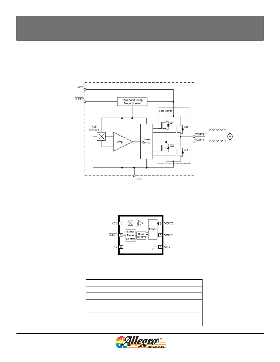
The A1441 is a full-bridge motor driver designed to drive low-voltage bipolar
brushless dc motors. Commutation of the motor is achieved by use of a single
Hall element sensor to detect the position of an alternating-pole ring magnet. A
high density merged Bipolar-CMOS semiconductor process allows the integra-
tion of the Hall element on the same IC as the motor control circuitry, providing
a single-chip solution for enhanced reliability. All necessary circuitry is incor-
porated within the device package, eliminating the need for any external support
components.
A micropower sleep mode can be enabled by an external signal, to reduce current
consumption for battery management in portable electronic devices. In addition,
the device offers an active function for motor braking.
The A1441 is optimized for vibration motor applications such as cellular phones,
pagers, electronic toothbrushes, and hand-held video game controllers. These
devices also drive low power fan motors designed with cogging plates.
The small package outline and low profile make this device ideally suited for use
in applications where printed circuit board area and component headroom are at
a premium. It is available in a lead (Pb) free (leadframe plating 100% matte tin)
6-pin MLP microleadframe package for surface mount, with exposed pad for
enhanced thermal dissipation.
Low-Voltage Full-Bridge Brushless DC Motor Driver
with Hall Element Commutation
Use the following complete part numbers when ordering:
Features and Benefits
Part Number
Package
Packing
A1441SELLT-T
2
◊
2
◊
0.50 mm
7-in. Reel, 3000 pieces/reel
Package EL, 6-pin Surface Mount MLP
1
2
3
6
5
4
Approximate Actual Size
Package EL
2
◊
2 mm
2
A1441-DS
Worcester, Massachusetts 01615-0036 (508) 853-5000
115 Northeast Cutoff, Box 15036
www.allegromicro.com
Allegro MicroSystems, Inc.
Low-Voltage Full-Bridge Brushless DC Motor Driver with Hall Element Commutation
A1441
Functional Block Diagram
Package EL, 2 ◊ 2 mm, 6-pin Surface Mount MLP
Terminal List Table
Pin
Name
Function
1
VDD
Supply voltage
2
ØSØ ØLØ ØEØ ØEØ ØPØ
Toggle Sleep/Enabled modes
3
NC
No connection
4
GND
Ground
5
VOUT1
First output
6
VOUT2
Second output

3
A1441-DS
Worcester, Massachusetts 01615-0036 (508) 853-5000
115 Northeast Cutoff, Box 15036
www.allegromicro.com
Allegro MicroSystems, Inc.
Low-Voltage Full-Bridge Brushless DC Motor Driver with Hall Element Commutation
A1441
DEVICE CHARACTERISTICS over the voltage and temperature operating range, unless otherwise specified
Characteristics
Symbol
Test Conditions
Min.
Typ.
Max.
Units
Supply Voltage
V
DD
Running
2.0
≠
4.0
V
Total Output Saturation Voltage
1
V
OUT(Sat)
I
LOAD
= 70 mA, V
DD
= 3.6 V
≠
300
≠
mV
I
LOAD
= 100 mA, V
DD
= 3.6 V
≠
450
≠
mV
I
LOAD
= 70 mA, V
DD
= 2.2 V
≠
400
≠
mV
Sleep Mode Supply Current
I
DD(Sleep)
≠
≠
10
A
Load Current Rise Time
2
t
r(ILOAD)
V
DD
= 3.6 V
≠
10
≠
s
Chopping Settling Time
3
t
s(CHOP)
≠
30
≠
s
ØSØ ØLØ ØEØ ØEØ ØPØ Input Threshold
V
INLO
≠
≠
0.5
V
V
INHI
V
DD
≠0.7
≠
≠
V
ØSØ ØLØ ØEØ ØEØ ØPØ Input Current
I
IN
≠
≠
1
A
Crossover Dead Time
4
t
DT
VOUT switching
≠
2
≠
s
Restart Delay
5
t
RS
≠
100
≠
ms
Magnetic Switchpoints
B
OP
≠
35
75
G
B
RP
≠75
≠35
≠
G
B
HYS
B
OP
≠ B
RP
;
B
OP
> B
RP
≠
70
≠
G
Startup Polarity
V
OUT1
B<Brp
LOW
≠
B>Bop
HIGH
≠
V
OUT2
B<Brp
HIGH
≠
B>Bop
LOW
≠
1
Either
V
OUT(Sat)
= V
Q1(Sat)
+ V
Q4(Sat)
or V
OUT(Sat)
= V
Q2(Sat)
+ V
Q3(Sat)
.
Total output saturation voltage is a sum of the voltages
across the active output transistors.
2
Time period required for current to change from 10% to 90% of it's value.
3
Chopping settling time is the required time to have valid device output after power up of the device.
4
Crossover dead time is a time period during which all output transistors are switched off.
5
Restart delay is a time period during which only one pair of the output transistors is switched on.

4
A1441-DS
Worcester, Massachusetts 01615-0036 (508) 853-5000
115 Northeast Cutoff, Box 15036
www.allegromicro.com
Allegro MicroSystems, Inc.
Low-Voltage Full-Bridge Brushless DC Motor Driver with Hall Element Commutation
A1441
The products described herein are manufactured under one or
more of the following U.S. patents: 5,045,920; 5,264,783; 5,442,283;
5,389,889; 5,581,179; 5,517,112; 5,619,137; 5,621,319; 5,650,719;
5,686,894; 5,694,038; 5,729,130; 5,917,320; and other patents pend-
ing.
Allegro MicroSystems, Inc. reserves the right to make, from time to
time, such de par tures from the detail spec i fi ca tions as may be required
to permit improvements in the per for mance, reliability, or manufactur-
ability of its products. Before placing an order, the user is cautioned to
verify that the information being relied upon is current.
Allegro products are not authorized for use as critical components in
life-support devices or sys tems without express written approval.
The in for ma tion in clud ed herein is believed to be ac cu rate and reli-
able. How ev er, Allegro MicroSystems, Inc. assumes no re spon si bil i ty
for its use; nor for any in fringe ment of patents or other rights of third
parties which may result from its use.
Copyright © 2005, Allegro MicroSystems, Inc.
Package EL, 6-Pin MLP
1.100
MAX
.043
1.550
BSC
.061
0.32
MIN
.013
1
6
0.50
BSC
.020
1.100
0.850
.043
.033
0.32
0.20
.013
.008
1.550
1.300
.061
.051
0.35
0.15
.014
.006
0.50
BSC
.020
2.00
BSC
.079
0.55
0.45
.022
.018
0.05
0.00
.002
.000
0.15
REF
.006
R0.200
REF
.008
0.50
NOM
.020
0.15
MIN
.006
2.40
REF
.094
0.20
REF
.008
2
6
1
2
1
6
A
Dimensions in millimeters
U.S. Customary dimensions (in.)
in brackets, for reference only
A Pin index area
B Exposed thermal pad
C
D
Optional thermal vias,
0.30 [.012], pitch 1.2 [.047]
Typical pad layout; adjust as necessary to
meet application process requirements
C
D
B
1.00 .0394
E
E
1.00 .0394
E
Hall element (not to scale), controlling dimension
inches
E