 | –≠–ª–µ–∫—Ç—Ä–æ–Ω–Ω—ã–π –∫–æ–º–ø–æ–Ω–µ–Ω—Ç: A2580SLW | –°–∫–∞—á–∞—Ç—å:  PDF PDF  ZIP ZIP |
This versatile family of integrated circuits will work with many combina-
tions of logic- and load-voltage levels, meeting interface requirements beyond
the capabilities of standard logic buffers. Series UDN2580A and A2580SLW
source drivers can drive incandescent, LED, or vacuum fluorescent displays.
Internal transient-suppression diodes permit the drivers to be used with
inductive loads such as relays, solenoids, dc and stepping motors, and mag-
netic print hammers.
The Types UDN2580A and A2580SLW are high-current source drivers
used to switch the ground ends of loads that are directly connected to a -50 V
supply. Typical loads are telephone relays, PIN diodes, and LEDs.
The UDN2585A and A2585SLW are drivers designed for applications
requiring low output saturation voltages. Typical loads are low-voltage LEDs
and incandescent displays. The eight non-Darlington, 25 V outputs will
simultaneously sustain continuous load currents of -120 mA at ambient
temperatures to +70
∞C.
The UDN2588A and A2588SLW have separate logic and driver supply
lines. Their eight drivers can serve as an interface between positive logic
(TTL, CMOS, PMOS) or negative logic (NMOS) and either negative or split-
load supplies to -80 V.
These drivers are packaged in plastic DlPs (suffix A) or surface-mount-
able wide-body SOlCs (suffix LW), and are rated for operation over the
temperature range of -20
∞C to +85∞C.
FEATURES
I TTL, CMOS, PMOS, NMOS Compatible
I High Output-Current Rating
I Internal Transient Suppression
I Efficient Input/Output Structure
I Through-Hole and Surface-Mount Packages
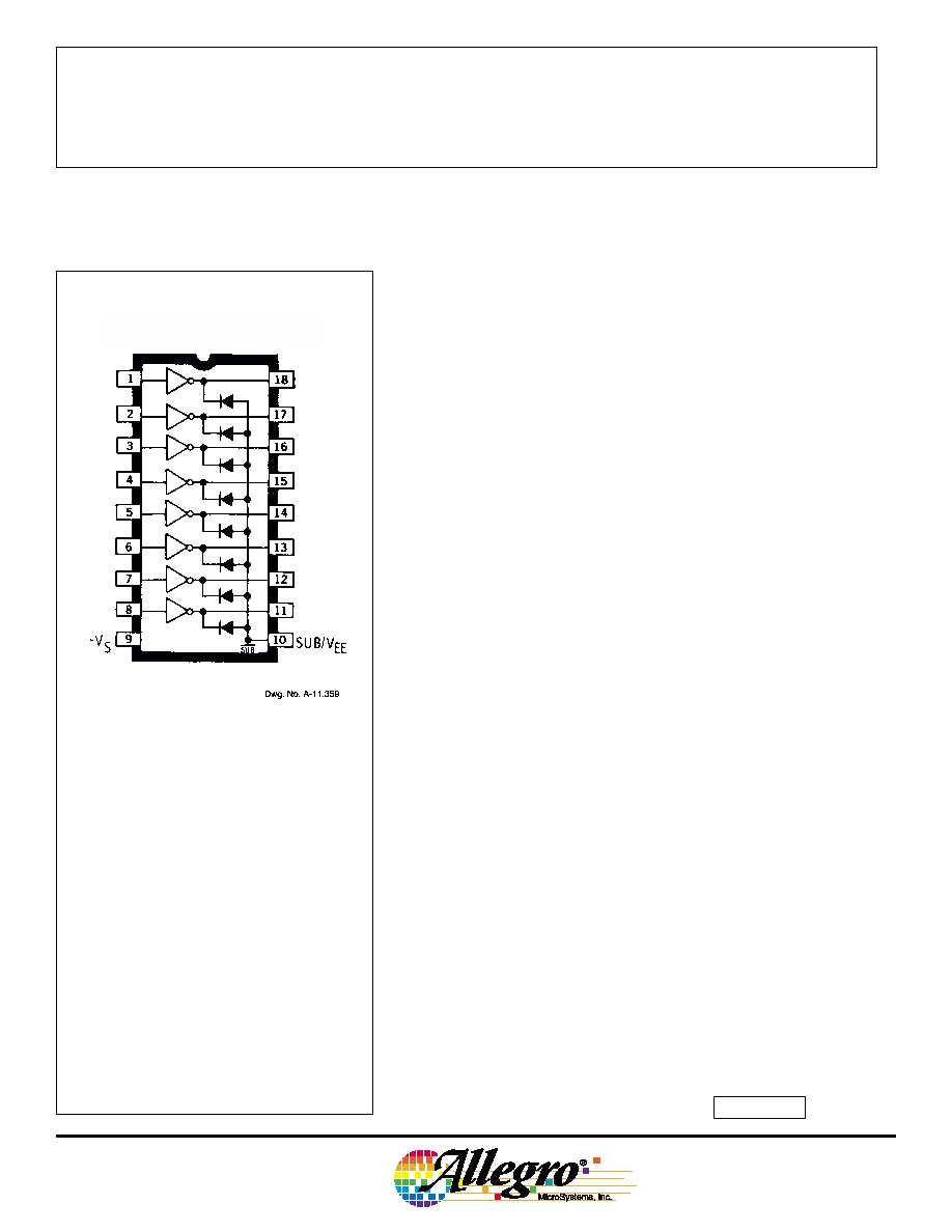
8-CHANNEL SOURCE DRIVERS
Always order by complete part number, e.g., UDN2580A .
Data Sheet
29316C*
UDN2580A and UDN2585A
ABSOLUTE MAXIMUM RATINGS
See next page.
2580, 2585,
AND
2588
2580, 2585,
AND
2588
8-CHANNEL
SOURCE DRIVERS
115 Northeast Cutoff, Box 15036
Worcester, Massachusetts 01615-0036 (508) 853-5000
2
ABSOLUTE MAXIMUM RATINGS
at 25
∞
C Free-Air Temperature for any one driver (unless otherwise noted).
UDN2580A
UDN2585A
UDN2588A
A2580SLW
A2585SLW
A2588SLW
Output Voltage, V
CE
50 V
25 V
80 V
Supply Voltage, V
S
(ref. sub.)
50 V
25 V
80 V
Supply Voltage, V
CC
(ref. sub.)
--
--
80 V
Input Voltage, V
IN
(ref. V
S
)
-30 V
-20 V
-30 V
Total Output Current, (l
C
+ I
S
)
-500 mA
-250 mA
-500 mA
Substrate Current I
SUB
3.0 A
2.0 A
3.0 A
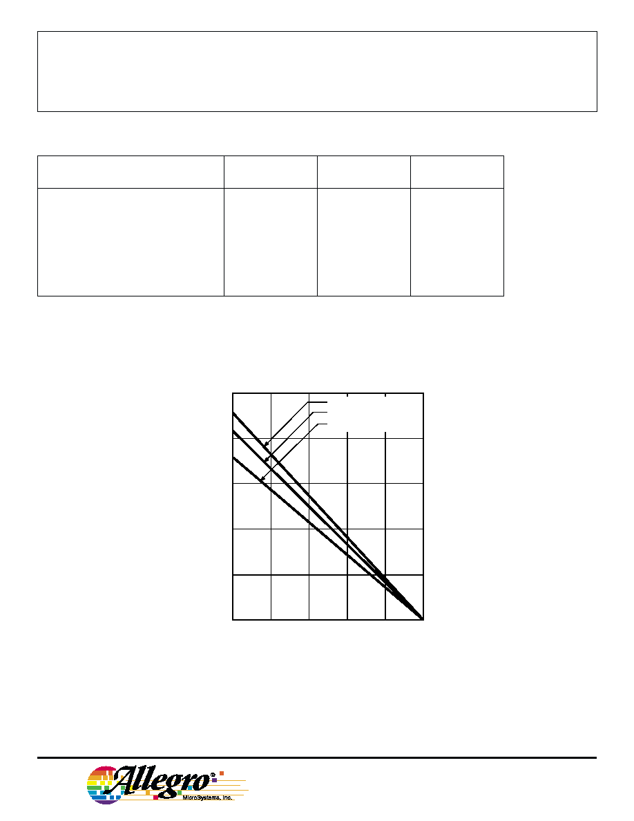
Package Power Dissipation, P
D
(single output) . . . . . . . . . . . . . . . . . . . . . . . . . . . . . . . . . . . . . . . . . . . . . . . . . . . . . . . . . . . . . . . . . 1.0 W
(total package) . . . . . . . . . . . . . . . . . . . . . . . . . . . . . . . . . . . . . . . . . . . . . . . . . . . . . . . . . . . . See Graph
Operating Temperature Range, T
A
. . . . . . . . . . . . . . . . . . . . . . . . . . . . . . . . . . . . . . . . . . . . . . . . . . . . . . . . . . . . . . . . . . . -20
∞
C to +85
∞
C
Storage Temperature Range, T
S
. . . . . . . . . . . . . . . . . . . . . . . . . . . . . . . . . . . . . . . . . . . . . . . . . . . . . . . . . . . . . . . . . . . .-55
∞
C to +150
∞
C
50
75
100
125
150
2.5
0.5
0
ALLOWABLE PACKAGE POWER DISSIPATION IN WATTS
AMBIENT TEMPERATURE IN
∞C
2.0
1.5
1.0
25
Dwg. GP-022-1
18-PIN DIP, R = 60
∞C/W
JA
20-PIN DIP, R = 55
∞C/W
JA
20-LEAD SOIC, R = 70
∞C/W
JA
W
Copyright © 1981, 2000 Allegro MicroSystems, Inc.

2580, 2585,
AND
2588
8-CHANNEL
SOURCE DRIVERS
www.allegromicro.com
3
TYPICAL OPERATING VOLTAGES
V
S
V
lN(ON)
V
lN(OFF)
V
CC
V
EE(MAX)
Device Types
0 V
-15 V to -3.6 V
-0.5 V to 0 V
NA
-25 V
UDN2585A & A2585SLW
-50 V
UDN2580A & A2580SLW
+5 V
0 V to +1.4 V
+4.5 V to +5 V
NA
-20 V
UDN2585A & A2585SLW
-45 V
UDN2580A & A2580SLW
5 V
-75 V
UDN2588A & A2588SLW
+12 V
0 V to +8.4 V
+11.5 V to +12 V
NA
-13 V
UDN2585A & A2585SLW
-38 V
UDN2580A & A2580SLW
12 V
-68 V
UDN2588A & A2588SLW
+15 V
0 V to +11.4 V
+14.5 V to +15 V
NA
-10V
UDN2585A & A2585SLW
-35 V
UDN2580A & A2580SLW
15 V
-65 V
UDN2588A & A2588SLW
NOTE: The substrate must be tied to the most negative point in the external circuit to maintain isolation between drivers and to provide
for normal circuit operation.
For simplification, these devices are characterized on the following pages with
specific voltages for inputs, logic supply (V
S
), load supply (V
EE
), and collector
supply (V
CC
). Typical use of the UDN2580A and A2580SLW is with negative-
referenced logic. The more common application of the UDN2585A, A2585SLW,
UDN2588A and A2588SLW are with positive-referenced logic supplies. In
application, the devices are capable of operation over a wide range of logic and
supply voltage levels:
2580, 2585,
AND
2588
8-CHANNEL
SOURCE DRIVERS
115 Northeast Cutoff, Box 15036
Worcester, Massachusetts 01615-0036 (508) 853-5000
4
Dwg. No. A-11,358
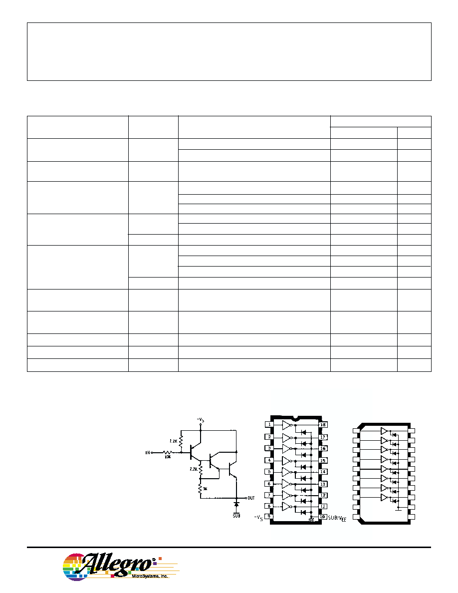
UDN2580A and A2580SLW
ELECTRICAL CHARACTERISTICS at T
A
= +25
∞
C, V
S
= 0 V, V
EE
= -45 V (unless otherwise noted).
Limits
Characteristic
Symbol
Test Conditions
Min.
Max.
Units
Output Leakage
I
CEX
V
lN
= -0.5 V, V
OUT
= V
EE
= -50 V
--
50
µA
Current
V
lN
= -0.4 V, V
OUT
= V
EE
= -50 V, T
A
= 70
∞C
--
100
µA
Output Sustaining
V
CE(SUS)
V
lN
= -0.4 V, I
OUT
= -25 mA, Note 1
35
--
V
Voltage
Output Saturation
V
CE(SAT)
V
lN
= -2.4 V, I
OUT
= -100 mA
--
1.8
V
Voltage
V
lN
= -3.0 V, I
OUT
= -225 mA
--
1.9
V
V
lN
= -3.6 V, I
OUT
= -350 mA
--
2.0
V
Input Current
I
IN(ON)
V
lN
= -3.6 V, I
OUT
= -350 mA
--
-500
µA
V
lN
= -15 V, I
OUT
= -350 mA
--
-2.1
mA
I
IN(OFF)
I
OUT
= -500
µA, T
A
= 70
∞C, Note 3
-50
--
µA
Input Voltage
V
IN(ON)
I
OUT
= -100 mA, V
CE
1.8 V, Note 4
--
-2.4
V
I
OUT
= -225 mA, V
CE
1.9 V, Note 4
--
-3.0
V
I
OUT
= -350 mA, V
CE
2.0 V, Note 4
--
-3.6
V
V
IN(OFF)
I
OUT
= -500
µA, T
A
= 70
∞C
-0.2
--
V
Clamp Diode
I
R
V
R
= 50 V, T
A
= 70
∞C
--
50
µA
Leakage Current
Clamp Diode
V
F
I
F
= 350 mA
--
2.0
V
Forward Voltage
Input Capacitance
C
IN
--
25
pF
Turn-On Delay
t
PHL
0.5 E
IN
to 0.5 E
OUT
--
5.0
µs
Turn-Off Delay
t
PLH
0.5 E
IN
to 0.5 E
OUT
--
5.0
µs
Dwg. PP-064
UDN2580A
A2580SLW
Dwg. No. A-11,359
PARTIAL SCHEMATIC
NOTES:
1.
Pulsed test, t
p
300 µs,
duty cycle
2%.
2.
Negative current is
defined as coming out of the
specified device pin.
3.
The I
IN(OFF)
current limit
guarantees against partial
turn-on of the output.
4.
The V
IN(ON)
voltage limit
guarantees a minimum
output source current per the
specified conditions.
5.
The substrate must
always be tied to the most
negative point and must be at
least 4.0 V below V
S
.
13
14
15
16
17
19
12
18
20
11
1
2
3
8
9
4
5
6
7
10
NC
NC
SUB/V
EE
SUB
+V
S
2580, 2585,
AND
2588
8-CHANNEL
SOURCE DRIVERS
www.allegromicro.com
5
UDN2585A and A2585SLW
ELECTRICAL CHARACTERISTICS at T
A
= +25
∞
C, V
S
= 0 V, V
EE
= -20 V (unless otherwise noted).
Limits
Characteristic
Symbol
Test Conditions
Min.
Max.
Units
Output Leakage
I
CEX
V
lN
= -0.5 V, V
OUT
= V
EE
= -25 V
--
50
µA
Current
V
lN
= -0.4 V, V
OUT
= V
EE
= -25 V, T
A
= 70
∞C
--
100
µA
Output Sustaining
V
CE(SUS)
V
lN
= -0.4 V, I
OUT
= -25 mA, Note 1
15
--
V
Voltage
Output Saturation
V
CE(SAT)
V
lN
= -4.6 V, I
OUT
= -60 mA
--
1.1
V
V
lN
= -4.6 V, I
OUT
= -120 mA
--
1.2
V
Input Current
I
IN(ON)
V
lN
= -4.6 V, I
OUT
= -120 mA
--
-1.6
mA
V
lN
= -14.6 V, I
OUT
= -120 mA
--
-5.0
mA
Input Voltage
V
IN(ON)
I
OUT
= -120 mA, V
CE
1.2 V, Note 3
--
-4.6
V
V
IN(OFF)
I
OUT
= -100
µA, T
A
= 70
∞C
-0.4
--
V
Clamp Diode
I
R
V
R
= 25 V, T
A
= 70
∞C
--
50
µA
Leakage Current
Clamp Diode
V
F
I
F
= 120 mA
--
2.0
V
Forward Voltage
Input Capacitance
C
IN
--
25
pF
Turn-On Delay
t
PHL
0.5 E
IN
to 0.5 E
OUT
--
5.0
µs
Turn-Off Delay
t
PLH
0.5 E
IN
to 0.5 E
OUT
--
5.0
µs
NOTES: 1. Pulsed test, t
p
300 µs, duty cycle 2%.
2. Negative current is defined as coming out of the specified device pin.
3. The V
IN(ON)
voltage limit guarantees a minimum output source current per the specified conditions.
4. The substrate must always be tied to the most negative point and must be at least 4.0 V below V
S
.
Voltage
Dwg. No. A-11,360
Dwg. PP-064
13
14
15
16
17
19
12
18
20
11
1
2
3
8
9
4
5
6
7
10
NC
NC
SUB/V
EE
SUB
+V
S
UDN2585A
A2585SLW
Dwg. No. A-11,359
PARTIAL SCHEMATIC