 | –≠–ª–µ–∫—Ç—Ä–æ–Ω–Ω—ã–π –∫–æ–º–ø–æ–Ω–µ–Ω—Ç: A2917 | –°–∫–∞—á–∞—Ç—å:  PDF PDF  ZIP ZIP |

The UDN2917EB motor driver is designed to drive both windings
of a bipolar stepper motor or bidirectionally control two dc motors. Both
bridges are capable of sustaining 45 V and include internal pulse-width modula-
tion (PWM) control of the output current to 1.5 A.
For PWM current control, the maximum output current is determined by the
user's selection of a reference voltage and sensing resistor. Two logic-level
inputs select output current limits of 0, 33%, 67%, or 100% of the maximum
level. A PHASE input to each bridge determines load current direction. Active-
low ENABLE inputs control the four drivers in each bridge.
The bridges include both ground clamp and flyback diodes for protection
against inductive transients. Internally generated delays prevent cross-over
currents when switching current direction. Special power-up sequencing is not
required. Thermal protection circuitry disables the outputs if the chip tempera-
ture exceeds safe operating limits.
The UDN2917EB is supplied in a 44-lead power PLCC for surface-mount
applications. Its batwing construction provides for maximum package power
dissipation in the smallest possible construction. The UDN2917EB is available
for operation from -40
∞C to +85∞C. To order, change the prefix from 'UDN' to
'UDQ'. This device is also available on special order for operation to +125
∞C.
2 9 1 7
DUAL FULL-BRIDGE
PWM MOTOR DRIVER
GND
GND
GND
GND
6
5
4
3
2
1
44
43
42
41
40
7
8
9
10
11
12
13
14
15
16
17
29
30
39
38
37
36
35
34
33
32
31
28
27
26
25
24
23
22
21
20
19
18
Dwg. PP-021
1
2
PWM 1
PWM 2
LOGIC SUPPLY
OUT
1A
E
1
SENSE
1
I
10
V
REF 1
PHASE
1
RC
1
ENABLE
1
I
11
OUT
1B
LOAD SUPPLY
E
OUT
2A
I
20
SENSE
2
V
REF 2
PHASE
2
RC
2
ENABLE
2
I
21
OUT
2B
2
1
2
EN
2
V
CC
V
BB
1
EN
ABSOLUTE MAXIMUM RATINGS
at T
J
+150∞C
Motor Supply Voltage, V
BB
.................... 45 V
Output Current, I
OUT
(t
w
20 µs) .....
±
1.75 A
(Continuous) ...............................
±
1.5 A
Logic Supply Voltage, V
CC
.................... 7.0 V
Logic Input Voltage Range,
V
IN
................................ -0.3 V to +7.0 V
Output Emitter Voltage, V
E
................... 1.0 V
Package Power Dissipation,
P
D
......................................... See Graph
Operating Temperature Range,
T
A
.................................. -20
∞
C to +85
∞
C
Storage Temperature Range,
T
S
................................ -55
∞
C to +150
∞
C
Output current rating may be limited by duty cycle,
ambient temperature, and heat sinking. Under any
set of conditions, do not exceed the specified peak
current rating or a junction temperature of +150
∞C.
Always order by complete part number: UDN2917EB .
Dwg. PP-021
Data Sheet
29319.22
FEATURES
I
1.5 A Continuous Output Current
I
45 V Output Sustaining Voltage
I
Internal Clamp Diodes
I
Digital Control of Output Current
I
Internal Thermal Shutdown Circuitry
I
Similar to Dual PBL3770
2917
DUAL FULL-BRIDGE
PWM MOTOR DRIVER
115 Northeast Cutoff, Box 15036
Worcester, Massachusetts 01615-0036 (508) 853-5000
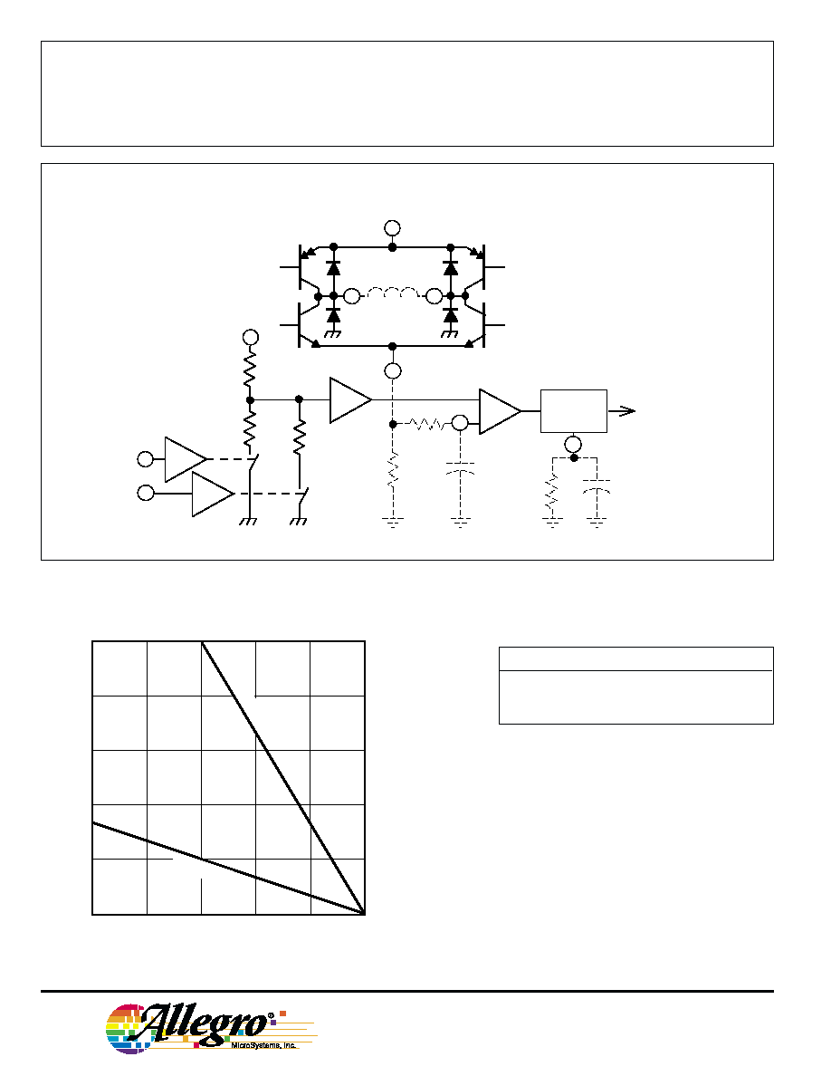
PWM CURRENT-CONTROL CIRCUITRY
TRUTH TABLE
Enable
Phase
Out
A
Out
B
L
H
H
L
L
L
L
H
H
X
Z
Z
X = Don't care
Z = High impedance
50
75
100
125
150
ALLOWABLE PACKAGE POWER DISSIPATION IN WATTS
TEMPERATURE IN
∞C
25
Dwg. GP-020B
12.5
2.5
0
10
7.5
5.0
R = 30
∞C/W
JA
R
=
6∞
C
/W
JT
V
REF
Dwg. EP-007-2A
V
BB
SENSE
ONE
SHOT
SOURCE
DISABLE
RC
≠
+
I
0
I
1
˜10
E
OUT A
OUTB
CHANNEL 1
PIN NUMBERS
SHOWN.
RC
R
S
R
T
C
C
C
T
22
20 k
40 k
10 k
3
6
5
4
41
2
1
44
Copyright © 1991, 2000 Allegro MicroSystems, Inc.

2917
DUAL FULL-BRIDGE
PWM MOTOR DRIVER
www.allegromicro.com
Limits
(at trip point)
ELECTRICAL CHARACTERISTICS at T
A
= +25
∞
C, V
BB
= 45 V, V
CC
= 5.0 V, V
REF
= 5.0 V (unless
otherwise noted).
Characteristic
Symbol
Test Conditions
Min.
Typ.
Max.
Units
Output Drivers (OUT
A
or OUT
B
)
Motor Supply Range
V
BB
10
--
45
V
Output Leakage Current
I
CEX
V
OUT
= V
BB
--
<1.0
50
µA
V
OUT
= 0
--
<-1.0
-50
µA
Output Sustaining Voltage
V
CE(sus)
I
OUT
=
±1.5 A, L = 3.5 mH
45
--
--
V
Output Saturation Voltage
V
CE(SAT
)
Sink Driver, I
OUT
= +1.0 A*
--
0.5
0.7
V
Sink Driver, I
OUT
= +1.5 A*
--
0.8
1.0
V
Source Driver, I
OUT
= -1.0 A*
--
1.8
1.9
V
Source Driver, I
OUT
= -1.5 A*
--
1.9
2.1
V
Clamp Diode Leakage Current
I
R
V
R
= 45 V
--
<1.0
50
µA
Clamp Diode Forward Voltage
V
F
I
F
= 1.5 A
--
1.6
2.0
V
Driver Supply Current
I
BB(ON)
Both Bridges On, No Load
--
9.0
12
mA
I
BB(OFF)
Both Bridges Off
--
4.0
6.0
mA
Control Logic
Input Voltage
V
IN(1)
All Inputs
2.4
--
--
V
V
IN(0)
All Inputs
--
--
0.8
V
Input Current
I
IN(1)
V
IN
= 2.4 V
--
<1.0
20
µA
I
IN(0)
V
IN
= 0.8 V
--
-3.0
-200
µA
Reference Voltage Range
V
REF
Operating
1.5
--
7.5
V
Current Limit Threshold
V
REF
/V
SENSE
I
0
= I
1
= 0.8 V
9.5
10
10.5
--
I
0
= 2.4 V, I
1
= 0.8 V
13.5
15
16.5
--
I
0
= 0.8 V, I
1
= 2.4 V
25.5
30
34.5
--
Thermal Shutdown Temp.
T
J
--
170
--
∞C
Total Logic Supply Current
I
CC(ON)
I
0
= I
1
= V
EN
= 0.8 V, No Load
--
90
105
mA
I
CC(OFF)
I
0
= I
1
= 2.4 V, No Load
--
10
12
mA
Negative current is defined as coming out of (sourcing) the specified device pin.
Typical Data is for design information only.
* Pulse test (<10 ms).
2917
DUAL FULL-BRIDGE
PWM MOTOR DRIVER
115 Northeast Cutoff, Box 15036
Worcester, Massachusetts 01615-0036 (508) 853-5000
+
≠
0
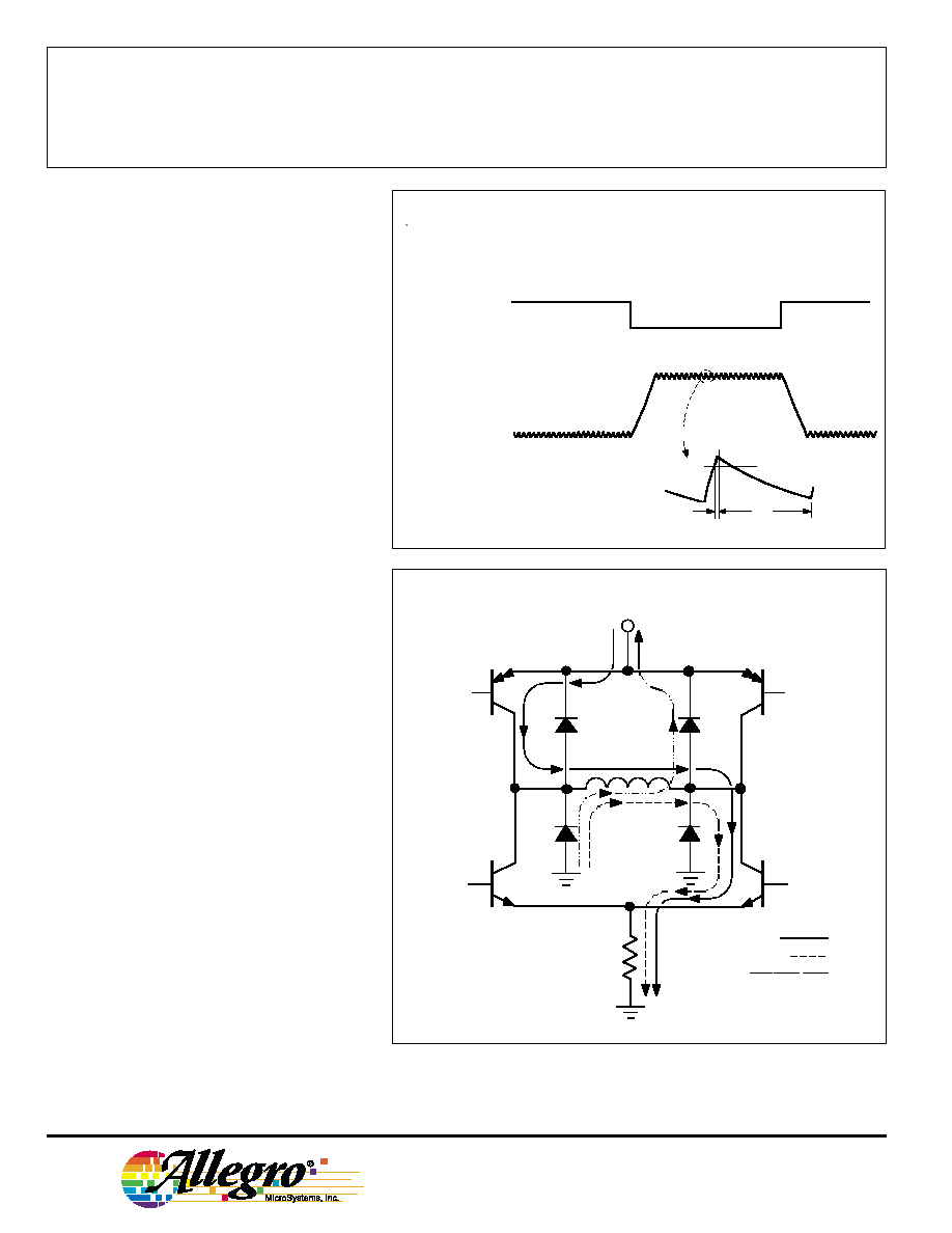
Dwg. WM-003-1A
V
PHASE
I
OUT
t
d
t
off
I
TRIP
APPLICATIONS INFORMATION
PWM CURRENT CONTROL
The UDN2917EB dual bridge is designed
to drive both windings of a bipolar stepper
motor. Output current is sensed and con-
trolled independently in each bridge by an
external sense resistor (R
S
), internal com-
parator, and monostable multivibrator.
When the bridge is turned on, current
increases in the motor winding and it is
sensed by the external sense resistor until the
sense voltage (V
SENSE
) reaches the level set
at the comparator's input:
I
TRIP
= V
REF
/10 R
S
The comparator then triggers the mon-
ostable which turns off the source driver of
the bridge. The actual load current peak will
be slightly higher than the trip point (espe-
cially for low-inductance loads) because of
the internal logic and switching delays. This
delay (t
d
) is typically 2
µs. After turn-off, the
motor current will normally decay, circulating
through the ground clamp diode and sink
transistor. The source driver's off time (and
therefore the magnitude of the current de-
crease) is determined by the monostable's
external RC timing components, where t
off
=
R
T
C
T
within the range of 20 k
to 100 k and
200 pF to 500 pF.
When the source driver is re-enabled, the
winding current (the sense voltage) is again
allowed to rise to the comparator's threshold.
This cycle repeats itself, maintaining the
average motor winding current at the desired
level.
Special circuitry has been included to
prevent runaway current control when the
fixed off time (t
off
) is set too short. This
circuitry prevents the source driver from being
re-enabled until the load current has decayed
to below the I
TRIP
level.
PWM OUTPUT CURRENT WAVEFORM
LOAD CURRENT PATHS
Dwg. EP-006-1
R S
BB
V
BRIDGE ON
SOURCE OFF
ALL OFF

2917
DUAL FULL-BRIDGE
PWM MOTOR DRIVER
www.allegromicro.com
Loads with high distributed capacitances may result in high turn-on
current peaks. This peak (appearing across R
S
) will attempt to trip the
comparator, resulting in erroneous current control or high-frequency
oscillations. An external R
C
C
C
low-pass filter may be needed to delay
the action of the comparator.
LOGIC CONTROL OF OUTPUT CURRENT
Two logic level inputs (I
0
and I
1
) allow digital selection of the motor
winding current at 100%, 67%, 33%, or 0% of the maximum level per
the table. The 0% output current condition turns off all drivers in the
bridge and can be used as an output enable function. These logic level
inputs greatly enhance the implementation of
µP-controlled drive
formats.
During half-step operations, the I
0
and I
1
inputs allow the
µP to
control the motor at a constant torque between all positions in an eight-
step sequence. This is accomplished by digitally selecting 100% drive
current when only one phase is on and 67% drive current when two
phases are on.
The logic control inputs can also be used to select a reduced
current level (and reduced power dissipation) for `hold' conditions
and/or increased current (and available torque) for start-up conditions.
GENERAL
To avoid excessive voltage spikes on the LOAD SUPPLY pin
(V
BB
), a large-value capacitor (
47 µF) should be connected from V
BB
to ground as close as possible to the device. Under no circumstances
should the voltage at LOAD SUPPLY exceed 45 V.
The PHASE input to each bridge determines the direction motor
winding current flows. An internally generated deadtime (approxi-
mately 3
µs) prevents crossover currents that can occur when switch-
ing the PHASE input.
All four drivers in the bridge output can be turned off (V
EN
2.4 V
or I
0
= I
1
2.4 V), resulting in a fast current decay through the internal
output clamp and flyback diodes. The fast current decay is desirable
in half-step and high-speed applications. All logic inputs float high; the
ENABLE input must be tied low if it is not used.
Varying the reference voltage (V
REF
) provides continuous control
of the peak load current for micro-stepping applications, within the
specified limits for V
REF
.
Thermal protection circuitry turns off all drivers when the junction
temperature reaches +170
∞C. It is only intended to protect the device
from failures due to excessive junction temperature and should not
imply that output short circuits are permitted. The output drivers are
re-enabled when the junction temperature cools to +145
∞C.
I
0
I
1
Output Current
L
L
V
REF
/10 R
S
= I
TRIP
H
L
V
REF
/15 R
S
=
2/3 I
TRIP
L
H
V
REF
/30 R
S
= 1/3 I
TRIP
H
H
0
CURRENT-CONTROL
TRUTH TABLE