 | –≠–ª–µ–∫—Ç—Ä–æ–Ω–Ω—ã–π –∫–æ–º–ø–æ–Ω–µ–Ω—Ç: A3212 | –°–∫–∞—á–∞—Ç—å:  PDF PDF  ZIP ZIP |
DFN/MLPD (EH)
Conceptual Data Sheet
Subject to Change Without Notice March 24, 2006
Description
The A 3211 and A3212 integrated circuits are ultra-sensitive,
pole in de pen dent Hall-effect switches with latched digital
output. These sensors are es pe cial ly suited for operation in
battery-operated, hand-held equip ment such as cellular and
cordless tele phones, pagers, and palmtop com put ers. A 2.5
volt to 3.5 volt operation and a unique clocking scheme reduce
the average op er at ing power requirements to less than 15
W
with a 2.75 volt supply.
Unlike other Hall-effect switches, either a north or south pole
of suf fi cient strength will turn the output on in the A3212,
and in the absence of a magnetic field, the output is off. The
A3211 provides an inverted output. The polarity independence
and minimal power requirements allow these devices to easily
replace reed switches for superior reliability and ease of
manufacturing, while eliminating the requirement for signal
conditioning.
Improved stability is made possible through chopper
stabilization (dynamic offset cancellation), which reduces the
residual offset voltage normally caused by device overmolding,
temperature de pen den cies, and thermal stress.
3211-DS, Rev. 3
Features and Benefits
Micropower operation
Operation with north or south pole
2.5 to 3.5 V battery operation
Chopper stabilized
Superior temperature stability
Extremely low switchpoint drift
Insensitive to physical stress
High ESD protection
Sol id-state reliability
Small size
Easily manufacturable with magnet pole independence
Micropower, Ultra-sensitive
Hall-ef fect Switches
Continued on the next page...
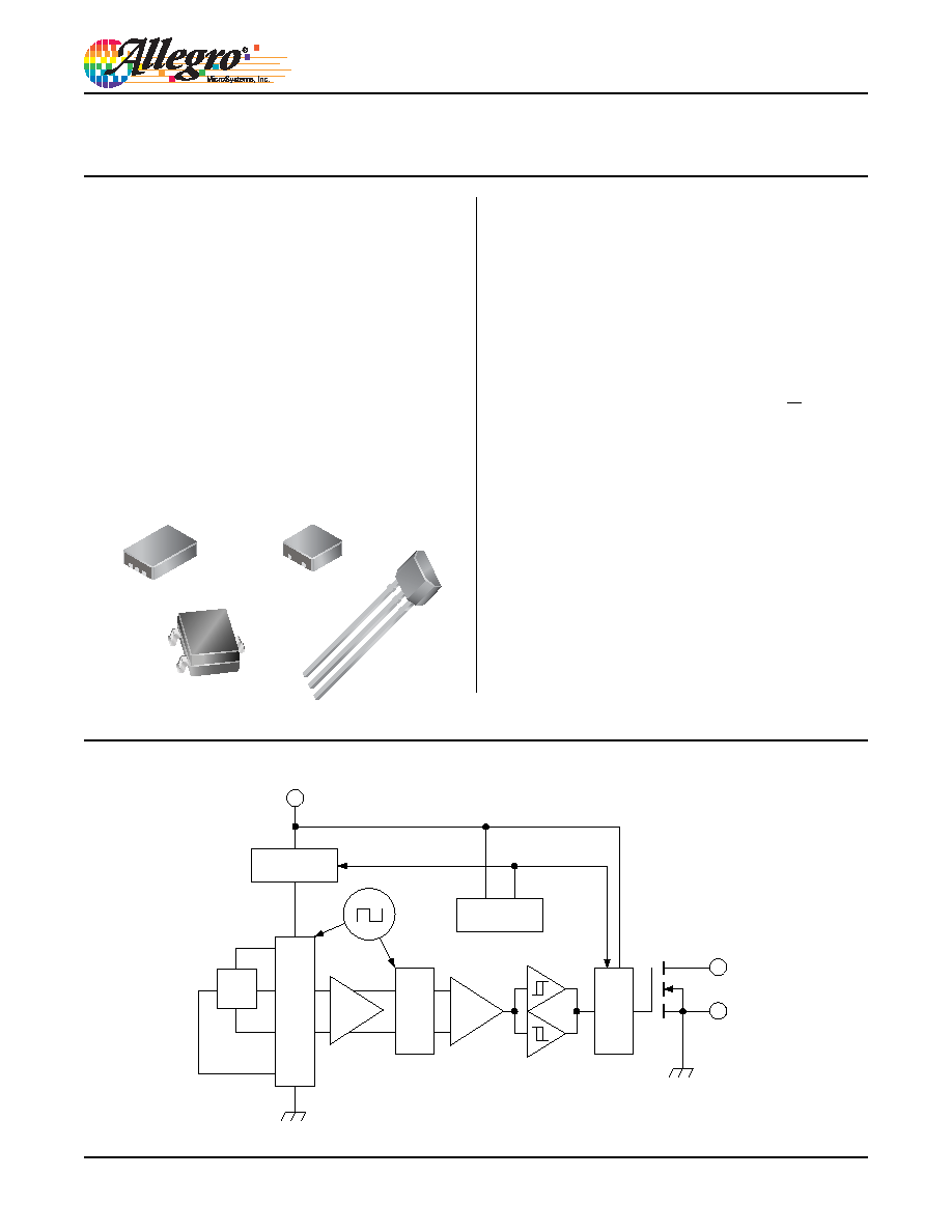
Packages:
Functional Block Diagram
Not to scale
A3211 and A3212
DFN/MLPD (EL)
SOT23W (LH)
SIP (UA)
TIMING
LOGIC
Dwg. FH-020-5
LATCH
GROUND
OUTPUT
SUPPLY
X
DYNAMIC
OFFSET CANCELLATION
SWITCH
SAMPLE
& HOLD
Micropower, Ultrasensitive
Hall Effect Switch
A3211
and
A3212
2
Allegro MicroSystems, Inc.
115 Northeast Cutoff, Box 15036
Worcester, Massachusetts 01615-0036 (508) 853-5000
www.allegromicro.com
Selection Guide
Part Number
Pb-free
1
Packing
2
(Units/Pack)
Package
Ambient
Temperature
T
A
(∞C)
A3211EEHLT≠T
Yes
Tape and Reel (3000)
Leadless Surface Mount
≠40 to 85
A3211EELLT≠T
Yes
Tape and Reel (3000)
A3211ELHLT≠T
Yes
Tape and Reel (3000)
3-Pin Surface Mount
A3212EEHLT≠T
Yes
Tape and Reel (3000)
Leadless Surface Mount
≠40 to 85
A3212EELLT≠T
Yes
Tape and Reel (3000)
A3212ELHLT≠T
Yes
Tape and Reel (3000)
3-Pin Surface Mount
A3212EUA≠T
Yes
Bulk Pack (500)
SIP-3 Through Hole, Straight Lead
A3212LLHLT≠T
Yes
Tape and Reel (3000)
3-Pin Surface Mount
≠40 to 150
A3212LUA≠T
Yes
Bulk Pack (500)
SIP-3 Through Hole, Straight Lead
1
Pb-based variants are being phased out of the product line. Certain variants cited in this footnote are in production but have been determined to be
NOT FOR NEW DESIGN. This classification indicates that sale of this device is currently restricted to existing customer applications. The variants
should not be purchased for new design applications because obsolescence in the near future is probable. Samples are no longer available. Status
change: May 1, 2006 for A3212EEHLT and A3212EUA, and October 31, 2005 for A3212LLHLT and A3212LUA.
2
Contact Allegro for additional packaging and handling options.
This device includes on a single silicon chip a Hall-voltage generator,
small-signal amplifier, chopper sta bi li za tion, a latch, and a MOSFET
output. Ad vanced BiCMOS processing is used to take advantage
of low-voltage and low-power requirements, component matching,
very low input-offset errors, and small component geometries.
Four package styles provide magnetically op
ti
mized
solutions for most ap
pli
ca
tions. Miniature low-
profile surface-mount package types EH and EL
(0.75 and 0.50 mm nominal height) are leadless, LH is a leaded low-
profile SMD, and UA is a three-lead SIP for through-hole mount ing.
Packages are available in lead (Pb) free versions (suffix, ≠T) with
100% matte tin plated leadframe. EL package for limited release,
engineering samples available.
Description (continued)
Absolute Maximum Ratings
Characteristic
Symbol
Notes
Rating
Units
Supply Voltage
V
DD
5
V
Magnetic Flux Density
B
Unlimited
G
Output Off Voltage
V
OUT
5
V
Output Current
I
OUT
1
mA
Operating Ambient Temperature
T
A
Range E
≠40 to 85
∫C
Range L
≠40 to 150
∫C
Maximum Junction Temperature
T
J
(max)
165
∫C
Storage Temperature
T
stg
≠65 to 170
∫C
Micropower, Ultrasensitive
Hall Effect Switch
A3211
and
A3212
3
Allegro MicroSystems, Inc.
115 Northeast Cutoff, Box 15036
Worcester, Massachusetts 01615-0036 (508) 853-5000
www.allegromicro.com
Package Suffix `UA' Pinning
(SIP)
Pinning is shown viewed from branded side.
Package Suffix `EH' Pinning
(Leadless Chip Carrier)
X
Dwg.
PH-016-2
SUPPLY
GROUND
OUTPUT
V
DD
GROUND
NO
CONNECTION
NO
CONNECTION
5
4
6
1
3
2
Dwg. PH-016
1
SUPPLY
V
DD
GROUND
3
2
OUTPUT
X
Package Suffix `LH' Pinning
(SOT23W)
Dwg. PH-016-1
SUPPLY
GROUND
OUTPUT
V
DD
1
2
3
Package Suffix `EL' Pinning
(Leadless Chip Carrier)
Dwg. PH-016-1
SUPPLY
GROUND
OUTPUT
V
DD
1
2
3
Micropower, Ultrasensitive
Hall Effect Switch
A3211
and
A3212
4
Allegro MicroSystems, Inc.
115 Northeast Cutoff, Box 15036
Worcester, Massachusetts 01615-0036 (508) 853-5000
www.allegromicro.com
ELECTRICAL CHARACTERISTICS
over operating voltage and temperature range (unless otherwise specified).
Characteristic
Symbol
Test Conditions
Limits
Min.
Typ.*
Max.
Units
Supply Voltage Range
V
DD
Operating
2.5
2.75
3.5
V
Output Leakage Current
I
OFF
V
OUT
= 3.5 V, Output off
≠
<1.0
1.0
A
Output On Voltage
V
OUT
I
OUT
= 1 mA, V
DD
= 2.75 V
≠
100
300
mV
Awake Time
t
awake
≠
45
90
s
Period
t
period
≠
45
90
ms
Duty Cycle
d.c.
≠
0.1
≠
%
Chopping Frequency
f
C
≠
340
≠
kHz
Supply Current
I
DD(EN)
Chip awake (enabled)
≠
≠
2.0
mA
I
DD(DIS)
Chip asleep (disabled)
≠
≠
8.0
A
I
DD(AVG)
V
DD
= 2.75 V
≠
5.1
10
A
V
DD
= 3.5 V
≠
6.7
10
A
* Typical data is at T
A
= 25∞C and V
DD
= 2.75 V, and is for design information only.

Micropower, Ultrasensitive
Hall Effect Switch
A3211
and
A3212
5
Allegro MicroSystems, Inc.
115 Northeast Cutoff, Box 15036
Worcester, Massachusetts 01615-0036 (508) 853-5000
www.allegromicro.com
3211 MAGNETIC CHARACTERISTICS
over operating voltage and temperature range (unless otherwise specified)
Characteristic
Symbol
Test Conditions
Limits
Min.
Typ.
Max.
Units
Operate Points
B
OPS
South pole to branded side; B > B
OP
, V
OUT
= Low (Output On)
≠
37
55
G
B
OPN
North pole to branded side; B > B
OP
, V
OUT
= Low (Output On)
≠55
≠40
≠
G
Release Points
B
RPS
South pole to branded side; B < B
RP
, V
OUT
= High (Output Off)
10
31
≠
G
B
RPN
North pole to branded side; B < B
RP
, V
OUT
= High (Output Off)
≠
≠34
≠10
G
Hysteresis
B
HYS
|B
OPx
- B
RPx
|
≠
5.9
≠
G
NOTES: 1. Negative flux densities are defined as less than zero (algebraic convention), i.e., -50 G is less than +10 G.
2.
B
OPx
= operate point (output turns on); B
RPx
= release point (output turns off).
3. Typical Data is at T
A
= +25∞C and V
DD
= 2.75 V and is for design information only.
4. 1 gauss (G) is exactly equal to 0.1 millitesla (mT).
3212 MAGNETIC CHARACTERISTICS
over operating voltage and temperature range (unless otherwise specified)
Characteristic
Symbol
Test Conditions
Limits
Min.
Typ.
Max.
Units
Operate Points
B
OPS
South pole to branded side; B > B
OP
, V
OUT
= High (Output Off)
≠
37
55
G
B
OPN
North pole to branded side; B > B
OP
, V
OUT
= High (Output Off)
≠55
≠40
≠
G
Release Points
B
RPS
South pole to branded side; B < B
RP
, V
OUT
= Low (Output On)
10
31
≠
G
B
RPN
North pole to branded side; B < B
RP
, V
OUT
= Low (Output On)
≠
≠34
≠10
G
Hysteresis
B
HYS
|B
OPx
- B
RPx
|
≠
5.9
≠
G
NOTES: 1. Negative flux densities are defined as less than zero (algebraic convention), i.e., -50 G is less than +10 G.
2.
B
OPx
= operate point (output turns off); B
RPx
= release point (output turns on).
3. Typical Data is at T
A
= +25∞C and V
DD
= 2.75 V and is for design information only.
4. 1 gauss (G) is exactly equal to 0.1 millitesla (mT).