A3245
A3245-DS, Rev. 1
Worcester, Massachusetts 01615-0036 (508) 853-5000
115 Northeast Cutoff, Box 15036
www.allegromicro.com
Allegro MicroSystems, Inc.
The A3245 integrated circuit is an omnipolar, ultrasensitive Hall-effect switch
with a digital output. This sensor has an integrated regulator permitting operation
to 24 V, making it the fi rst omnipolar switch available for operation to 24 V. This
device is especially suited for operation over extended temperature ranges, up
to +150∞C. Superior high-temperature performance is made possible through an
Allegro
Æ
patented dynamic offset cancellation, which reduces the residual offset
voltage normally caused by device overmolding, temperature excursions, and
thermal stress.
The A3245 Hall-effect switch includes the following on a single silicon chip:
voltage regulator, Hall-voltage generator, small-signal amplifi er, chopper stabiliza-
tion, Schmitt trigger, and a short circuit protected open-drain output. Advanced
BiCMOS wafer fabrication processing is used to take advantage of low-voltage
requirements, component matching, very low input-offset errors, and small com-
ponent geometries.
The omnipolar operation of the A3245 allows activation with either a north or
a south polarity fi eld of suffi cient strength. In the absence of a magnetic fi eld,
the output is off. This patented magnetic-polarity-independence feature makes
this device an excellent replacement for reed switches, with improved ease of
manufacturing, because the A3245 does not require manufacturers to orient their
magnets. These devices allow simple on/off switching in industrial, consumer, and
automotive applications.
The A3245 is rated for operation between the ambient temperatures ≠40∞C and
85∞C for the E temperature range, and ≠40∞C to 150∞C for the L temperature
range. The small geometries of the BiCMOS process allow these devices to be
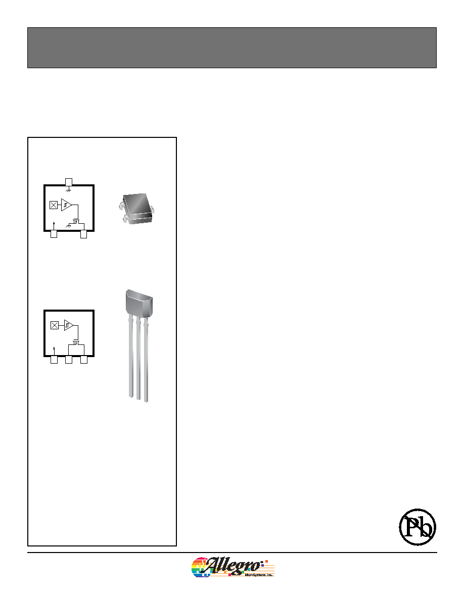
provided in ultrasmall packages. The package styles available provide magneti-
cally optimized solutions for most applications. Package LH is an SOT23W, a
miniature low-profi le surface-mount package, while package UA is a three-lead
ultramini SIP for through-hole mounting. Each package is available in a lead (Pb)
free version, with 100% matte tin plated leadframes.
AB SO LUTE MAX I MUM RAT INGS
Supply Voltage, V
CC
..........................................28 V
Reverse-Supply Voltage, V
RCC
........................≠18 V
Reverse-Supply Current, I
RCC
........................≠2 mA
Output Off Voltage, V
OUT
.................................. 28 V
Output Current, I
OUTSINK
........... Internally Limited
Magnetic Flux Density, B .........................Unlimited
Operating Temperature
Ambient,
T
A
, Range E.................. ≠40∫C to 85∫C
Ambient,
T
A
, Range L................ ≠40∫C to 150∫C
Maximum
Junction,
T
J(MAX)
......................165∫C
Storage Temperature, T
S
.................. ≠65∫C to 170∫C
Chopper-Stabilized
Omnipolar Hall-Effect Switches
Package LH, 3-pin Surface Mount
Features and Benefi ts
Package UA, 3-pin SIP
Omnipolar operation
Chopper stabilization
Superior temperature stability
Extremely low switchpoint drift
Insensitive to physical stress
Reverse battery protection
Output short circuit protection
Solid state reliability
Small size
Robust EMC capability
High ESD ratings (HBM)
1
3
2
VCC
GND
VOUT
1
2
3
VCC
VOUT
GND
1
2
3
1 2
3
2
A3245-DS, Rev. 1
Worcester, Massachusetts 01615-0036 (508) 853-5000
115 Northeast Cutoff, Box 15036
www.allegromicro.com
Allegro MicroSystems, Inc.
Chopper-Stabilized Omnipolar Hall Effect Switches
A3245
Product Selection Guide
Part Number
Pb-Free
Packing*
Mounting
Ambient, T
A
(∞C)
A3245ELHLT
≠
7-in. reel, 3000 pieces/reel
3-pin SOT23W surface mount
≠40 to 85
A3245ELHLT-T
Yes
A3245EUA
≠
Bulk, 500 pieces/bag
3-pin SIP through hole
A3245EUA-T
Yes
A3245LLHLT
≠
7-in. reel, 3000 pieces/reel
3-pin SOT23W surface mount
≠40 to 150
A3245LLHLT-T
Yes
A3245LUA
≠
Bulk, 500 pieces/bag
3-pin SIP through hole
A3245LUA-T
Yes
*Contact Allegro for additional packing options.
Functional Block Diagram
Regulator
GND
VCC
VOUT
Control
Current Limit
<1
Dyna
mic
O
ffse
t
Ca
nce
ll
a
t
i
o
n
Sam
p
le
and
H
old
To All Subcircuits
Amp
Low-Pass
Filter
Amp
Terminal List
Name
Description
Number
Package LH
Package UA
VCC
Connects power supply to chip
1
1
VOUT
Output from circuit
2
3
GND
Ground
3
2

3
A3245-DS, Rev. 1
Worcester, Massachusetts 01615-0036 (508) 853-5000
115 Northeast Cutoff, Box 15036
www.allegromicro.com
Allegro MicroSystems, Inc.
Chopper-Stabilized Omnipolar Hall Effect Switches
A3245
OPERATING CHARACTERISTICS
valid over full operating voltage and ambient temperature ranges, unless otherwise noted
Characteristic
Symbol
Test Conditions
Min.
Typ.
Max.
Units
Electrical Characteristics
Supply Voltage
1
V
CC
Operating, T
J
< 165∞C
3.6
≠
24
V
Output Leakage Current
I
OUTOFF
V
OUT
= 24 V, B < B
RP
≠
≠
10
A
Output On Voltage
V
OUT(SAT)
I
OUT
= 20 mA, B > B
OP
≠
≠
500
mV
Output Current Limit
I
OM
B > B
OP
30
≠
60
mA
Power-On Time
t
PO
V
CC
> V
CC(MIN)
≠
≠
50
s
Chopping Frequency
f
c
≠
200
≠
kHz
Output Rise Time
2
t
r
R
LOAD
= 820 , C
S
= 20 pF
≠
≠
1
s
Output Fall Time
2
t
f
R
LOAD
= 820 , C
S
= 20 pF
≠
≠
1
s
Supply Current
I
CCON
B > B
OP
≠
1.5
3.5
mA
I
CCOFF
B < B
RP
≠
1.5
3.5
mA
Reverse Battery Current
I
RCC
V
RCC
= ≠18 V
≠
≠
≠2
mA
Supply Zener Clamp Voltage
V
ZSupply
I
CC
= 6.5 mA; T
A
= 25∞C
28
≠
≠
V
Supply Zener Current
3
I
ZSupply
V
S
= 28 V
≠
≠
6.5
mA
Magnetic Characteristics
4
Operate Point
B
OPS
South pole adjacent to branded face of device
15
38
55
G
B
OPN
North pole adjacent to branded face of device
≠55
≠38
≠15
G
Release Point
B
RPS
South pole adjacent to branded face of device
5
20
50
G
B
RPN
North pole adjacent to branded face of device
≠50
≠20
≠5
G
Hysteresis
B
HYS
|B
OP
X
≠ B
RP
X
|
5
18
30
G
1
Maximum voltage must be adjusted for power dissipation and junction temperature, see
Power Derating
section.
2
C
S
= oscilloscope probe capacitance.
3
Maximum current limit is equal to the maximum I
CC(MAX)
+ 3 mA.
4
Magnetic fl ux density, B, is indicated as a negative value for north-polarity magnetic fi elds, and as a positive value for south-polarity magnetic fi elds.
This so-called algebraic convention supports arithmetic comparison of north and south polarity values, where the relative strength of the fi eld is indicated
by the absolute value of B, and the sign indicates the polarity of the fi eld (for example, a ≠100 G fi eld and a 100 G fi eld have equivalent strength, but
opposite polarity).
DEVICE QUALIFICATION PROGRAM
Contact Allegro for information.
EMC (Electromagnetic Compatibility) REQUIREMENTS
Contact Allegro for information.

4
A3245-DS, Rev. 1
Worcester, Massachusetts 01615-0036 (508) 853-5000
115 Northeast Cutoff, Box 15036
www.allegromicro.com
Allegro MicroSystems, Inc.
Chopper-Stabilized Omnipolar Hall Effect Switches
A3245
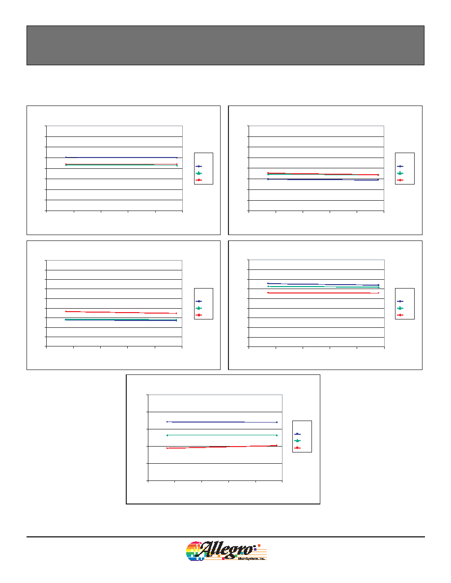
Electrical Characteristic Data
T
A
(∞C)
Supply Current (On) versus Ambient Temperature
V
CC
(V)
I
CCON
(mA)
24
3.6
T
A
(∞C)
Supply Current (Off) versus Ambient Temperature
V
CC
(V)
I
CCOFF
(mA)
24
3.6
T
A
(∞C)
Output Voltage (On) versus Ambient Temperature
V
CC
(V)
V
OUT(SA
T)
(mV)
24
3.6
Supply Current (On) versus Supply Voltage
T
A
(∞C)
I
CCON
(mA)
V
CC
(V)
≠40
25
150
Supply Current (Off) versus Supply Voltage
T
A
(∞C)
I
CCOFF
(mA)
V
CC
(V)
≠40
25
150
Output Voltage (On) versus Supply Voltage
T
A
(∞C)
V
OUT(SA
T)
(mV)
V
CC
(V)
≠40
25
150
0
1.0
2.0
3.0
4.0
5.0
0
1.0
2.0
3.0
4.0
5.0
0
1.0
2.0
3.0
4.0
5.0
0
1.0
2.0
3.0
4.0
5.0
≠50
0
50
100
150
0
5
10
15
20
25
≠50
0
50
100
150
0
5
10
15
20
25
≠50
0
50
100
150
0
5
10
15
20
25
0
50
200
250
100
150
300
350
400
450
500
0
50
200
250
100
150
300
350
400
450
500

5
A3245-DS, Rev. 1
Worcester, Massachusetts 01615-0036 (508) 853-5000
115 Northeast Cutoff, Box 15036
www.allegromicro.com
Allegro MicroSystems, Inc.
Chopper-Stabilized Omnipolar Hall Effect Switches
A3245
V
CC
(V)
24
3.6
T
A
(∞C)
V
CC
(V)
24
3.6
V
CC
(V)
24
3.6
Operate Point (South) versus Ambient Temperature
B
OPS
(G)
T
A
(∞C)
Release Point (North) versus Ambient Temperature
B
RPN
(G)
T
A
(∞C)
Hysteresis versus Ambient Temperature
B
HYS
(G)
T
A
(∞C)
V
CC
(V)
24
3.6
T
A
(∞C)
V
CC
(V)
24
3.6
Operate Point (North) versus Ambient Temperature
B
OPN
(G)
T
A
(∞C)
Release Point (South) versus Ambient Temperature
B
RPS
(G)
T
A
(∞C)
≠50
0
50
100
150
≠50
0
50
100
150
≠50
0
50
100
150
≠50
0
50
100
150
≠50
0
50
100
150
15
20
25
30
35
40
45
50
55
-50
-45
-40
-35
-30
-25
-20
-15
-10
-5
5
10
15
20
25
30
5
10
15
20
25
30
35
40
45
50
-55
-50
-45
-40
-35
-30
-25
-20
-15
Magnetic Characteristic Data
Continued on the next page...
6
A3245-DS, Rev. 1
Worcester, Massachusetts 01615-0036 (508) 853-5000
115 Northeast Cutoff, Box 15036
www.allegromicro.com
Allegro MicroSystems, Inc.
Chopper-Stabilized Omnipolar Hall Effect Switches
A3245
V
CC
(V)
Operate Point (South) versus Supply Voltage
B
OPS
(G)
Release Point (South) versus Supply Voltage
B
RPS
(G)
V
CC
(V)
Hysteresis versus Supply Voltage
B
HYS
(G)
V
CC
(V)
V
CC
(V)
Operate Point (North) versus Supply Voltage
B
OPN
(G)
Release Point (North) versus Supply Voltage
B
RPN
(G)
V
CC
(V)
T
A
(∞C)
≠40
25
150
T
A
(∞C)
≠40
25
150
T
A
(∞C)
≠40
25
150
T
A
(∞C)
≠40
25
150
T
A
(∞C)
≠40
25
150
0
5
10
15
25
20
0
5
10
15
25
20
0
5
10
15
25
20
0
5
10
15
25
20
0
5
10
15
25
20
15
20
25
30
35
40
45
50
55
-50
-45
-40
-35
-30
-25
-20
-15
-10
-5
5
10
15
20
25
30
5
10
15
20
25
30
35
40
45
50
-55
-50
-45
-40
-35
-30
-25
-20
-15
Magnetic Characteristic Data (Continued)
7
A3245-DS, Rev. 1
Worcester, Massachusetts 01615-0036 (508) 853-5000
115 Northeast Cutoff, Box 15036
www.allegromicro.com
Allegro MicroSystems, Inc.
Chopper-Stabilized Omnipolar Hall Effect Switches
A3245
THERMAL CHARACTERISTICS may require derating at maximum conditions, see application information
Characteristic
Symbol
Test Conditions
Value
Units
Package Thermal Resistance
R
JA
Package LH-3, 1-layer PCB with copper limited to
solder pads
110
∫C/W
Package LH-3, 2-layer PCB with 0.926 in
2
on each
side, connected by thermal vias
228
∫C/W
Package UA, 1-layer PCB with copper limited to
solder pads
165
∫C/W
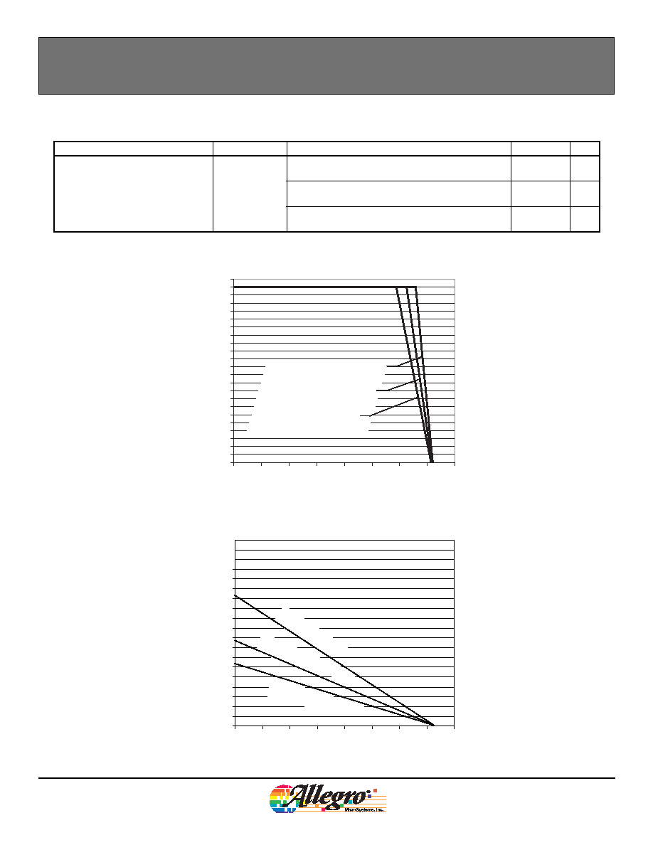
Power Derating Curve
2
3
4
5
6
7
8
9
10
11
12
13
14
15
16
17
18
19
20
21
22
23
24
25
20
40
60
80
100
120
140
160
180
Temperature (∞C)
M
a
x
i
mu
m A
l
l
o
w
a
b
l
e
V
CC
(V
)
1-layer PCB, Package LH
(R
JA
= 110 ∞C/W)
1-layer PCB, Package UA
(R
JA
= 165 ∞C/W)
2-layer PCB, Package LH
(R
JA
= 228 ∞C/W)
V
CC(min)
V
CC(max)
0
100
200
300
400
500
600
700
800
900
1000
1100
1200
1300
1400
1500
1600
1700
1800
1900
20
40
60
80
100
120
140
160
180
Temperature (∞C)
Power
D
is
s
i
p
a
t
i
o
n
,
P
D
(m
W)
Power Dissipation versus Ambient Temperature
(R
JA
= 165
∫C/W)
1-layer
PCB,
Packa
ge UA
(R
JA
= 228 ∫C/
W)
2-layer
PCB, Package
LH
(R
JA
= 110
∫C/W)
1-layer
PCB,
Package
LH
8
A3245-DS, Rev. 1
Worcester, Massachusetts 01615-0036 (508) 853-5000
115 Northeast Cutoff, Box 15036
www.allegromicro.com
Allegro MicroSystems, Inc.
Chopper-Stabilized Omnipolar Hall Effect Switches
A3245
Functional Description
B
OPS
B
OPN
B
RPN
B
RPS
B
HYS
B
HYS
V
S
V
OUT
V
OUT(SAT)
Switch
to
Low
Switch
to
Low
Switch
to
High
Switch
to
High
B+
B≠
V+
0
0
VCC
V
S
Sensor Output
GND
VOUT
R
LOAD
A3245
0.1 F
C
BYP
Operation
The output of this device switches low (turns on) when a mag-
netic fi eld perpendicular to the Hall sensor exceeds the operate
point, B
OPS
(or is less than B
OPN
). After turn-on, the output
voltage is V
OUT(SAT)
. The output transistor is capable of sink-
ing current up to the short circuit current limit, I
OM
, which is a
minimum of 30 mA. When the magnetic fi eld is reduced below
the release point, B
RPS
(or increased above B
RPN
), the device
output switches high (turns off). The difference in the magnetic
operate and release points is the hysteresis, B
HYS
, of the device.
This built-in hysteresis allows clean switching of the output even
in the presence of external mechanical vibration and electrical
noise.
Powering-on the device in a hysteresis region, between B
OPX
and B
RPX
, allows an indeterminate output state. The correct state
is attained after the fi rst excursion beyond B
OPX
or B
RPX
.
Applications
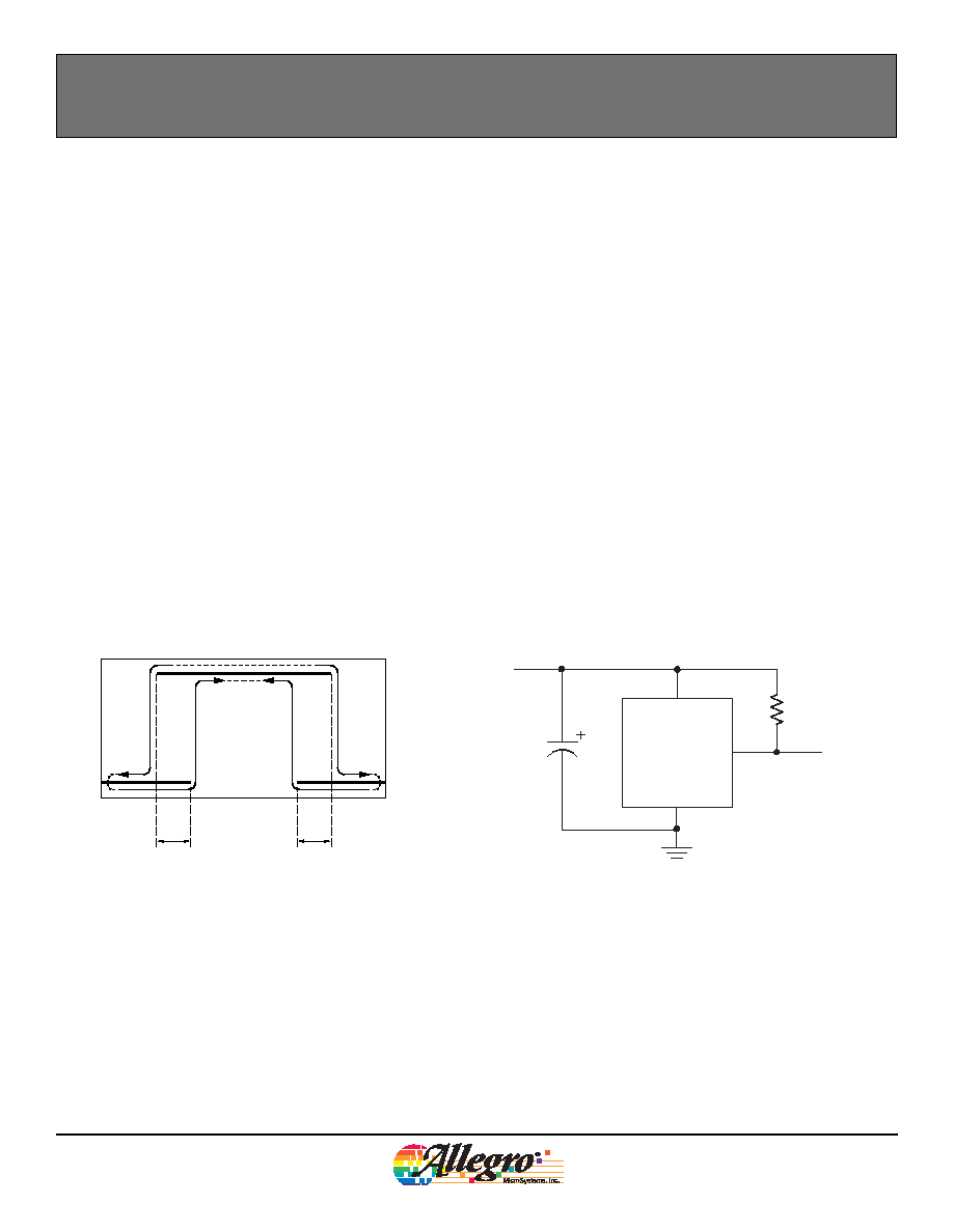
It is strongly recommended that an external bypass capacitor be
connected (in close proximity to the Hall sensor) between the
supply and ground of the device to reduce both external noise
and noise generated by the chopper stabilization technique. As is
shown in Panel B of fi gure 1, a 0.1F capacitor is typical.
Omnipolar switches allow operation with either a north pole or
south pole magnet orientation, enhancing product manufactur-
ability with the device.
Extensive applications information on magnets and Hall-effect
sensors is available in:
∑ Hall-Effect IC Applications Guide, AN27701,
∑ Hall-Effect Devices: Gluing, Potting, Encapsulating, Lead
Welding and Lead Forming, AN27703.1
∑ Soldering Methods for Allegro's Products ≠ SMT and Through-
Hole, AN26009
All are provided in Allegro Electronic Data Book, AMS-702 and
the Allegro Web site: www.allegromicro.com
Figure 1: Switching Behavior of Omnipolar Switches.
In Panel A,
on the horizontal axis, the B+ direction indicates increasing south polarity
magnetic fi eld strength, and the B≠ direction indicates decreasing south polarity fi eld strength (including the case of increasing north
polarity). This behavior can be exhibited when using a circuit such as that shown in panel B.
(A)
(B)
9
A3245-DS, Rev. 1
Worcester, Massachusetts 01615-0036 (508) 853-5000
115 Northeast Cutoff, Box 15036
www.allegromicro.com
Allegro MicroSystems, Inc.
Chopper-Stabilized Omnipolar Hall Effect Switches
A3245
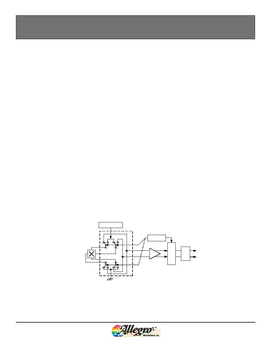
Figure 2. Chopper Stabilization Circuit (Dynamic Quadrature Offset Cancellation)
Amp
Regulator
Clock/Logic
Hall Element
Sa
mp
le
an
d
Ho
ld
Lo
w-P
a
s
s
Filte
r
Chopper Stabilization Technique
When using Hall-effect technology, a limiting factor for
switchpoint accuracy is the small signal voltage developed
across the Hall element. This voltage is disproportionally small
relative to the offset that can be produced at the output of the
Hall sensor. This makes it diffi cult to process the signal while
maintaining an accurate, reliable output over the specifi ed oper-
ating temperature and voltage ranges.
Chopper stabilization is a unique approach used to minimize
Hall offset on the chip. The patented Allegro technique, namely
Dynamic Quadrature Offset Cancellation, removes key sources
of the output drift induced by thermal and mechanical stresses.
This offset reduction technique is based on a signal modulation-
demodulation process. The undesired offset signal is separated
from the magnetic-fi eld-induced signal in the frequency domain,
through modulation. The subsequent demodulation acts as a
modulation process for the offset, causing the magnetic-fi eld-
induced signal to recover its original spectrum at baseband,
while the dc offset becomes a high-frequency signal. The mag-
netic-fi eld-induced signal then can pass through a low-pass fi lter,
while the modulated dc offset is suppressed. This confi guration
is illustrated in fi gure 2.
The chopper stabilization technique uses a 200 kHz high-fre-
quency clock. For demodulation process, a sample and hold
technique is used, where the sampling is performed at twice the
chopper frequency (400 kHz). This high-frequency operation
allows a greater sampling rate, which results in higher accuracy
and faster signal-processing capability. This approach desensi-
tizes the chip to the effects of thermal and mechanical stresses,
and produces devices that have extremely stable quiescent Hall
output voltages and precise recoverability after temperature
cycling. This technique is made possible through the use of a
BiCMOS process, which allows the use of low-offset, low-noise
amplifi ers in combination with high-density logic integration and
sample-and-hold circuits.
The repeatability of magnetic-fi eld-induced switching is affected
slightly by a chopper technique. However, the Allegro high-
frequency chopping approach minimizes the affect of jitter and
makes it imperceptible in most applications. Applications that
are more likely to be sensitive to such degradation are those
requiring precise sensing of alternating magnetic fi elds; for
example, speed sensing of ring-magnet targets. For such applica-
tions, Allegro recommends its digital sensor families with lower
sensitivity to jitter. For more information on those devices,
contact your Allegro sales representative.

10
A3245-DS, Rev. 1
Worcester, Massachusetts 01615-0036 (508) 853-5000
115 Northeast Cutoff, Box 15036
www.allegromicro.com
Allegro MicroSystems, Inc.
Chopper-Stabilized Omnipolar Hall Effect Switches
A3245
The device must be operated below the maximum junction
temperature of the device, T
J(max)
. Under certain combinations of
peak conditions, reliable operation may require derating sup-
plied power or improving the heat dissipation properties of the
application. This section presents a procedure for correlating
factors affecting operating T
J
. (Thermal data is also available on
the Allegro MicroSystems Web site.)
The Package Thermal Resistance, R
JA
, is a fi gure of merit sum-
marizing the ability of the application and the device to dissipate
heat from the junction (die), through all paths to the ambient air.
Its primary component is the Effective Thermal Conductivity,
K, of the printed circuit board, including adjacent devices and
traces. Radiation from the die through the device case, R
JC
, is
relatively small component of R
JA
. Ambient air temperature,
T
A
, and air motion are signifi cant external factors, damped by
overmolding.
The effect of varying power levels (Power Dissipation, P
D
), can
be estimated. The following formulas represent the fundamental
relationships used to estimate T
J
, at P
D
.
P
D
= V
IN
◊
I
IN
(1)
T = P
D
◊
R
JA
(2)
T
J
= T
A
+ T
(3)
For example, given common conditions such as: T
A
= 25∞C,
V
CC
= 12 V, I
CC
= 1.5 mA, and R
JA
= 165 ∞C/W, then:
P
D
= V
CC
◊
I
CC
= 12 V
◊
1.5 mA = 18 mW
T = P
D
◊
R
JA
= 18 mW
◊
165 ∞C/W = 3∞C
T
J
= T
A
+
T = 25∞C + 3∞C = 28∞C
A worst-case estimate, P
D(max)
, represents the maximum allow-
able power level (V
CC(max)
, I
CC(max)
), without exceeding T
J(max)
,
at a selected R
JA
and T
A
.
Example: Reliability for V
CC
at T
A
=
150∞C, package LH, using a
low-K PCB.
Observe the worst-case ratings for the device, specifi cally:
R
JA
=
228 ∞C/W, T
J(max)
=
165∞C, V
CC(max)
=
24 V, and
I
CC(max)
=
5
mA.
Calculate the maximum allowable power level, P
D(max)
. First,
invert equation 3:
T
max
= T
J(max)
≠ T
A
= 165
∞C
≠
150
∞C = 15
∞C
This provides the allowable increase to T
J
resulting from internal
power dissipation. Then, invert equation 2:
P
D(max)
=
T
max
˜ R
JA
= 15∞C ˜ 228 ∞C/W = 65.8 mW
Finally, invert equation 1 with respect to voltage:
V
CC(est)
= P
D(max)
˜ I
CC(max)
= 65.8 mW ˜ 5 mA = 13.2 V
The result indicates that, at T
A
, the application and device can
dissipate adequate amounts of heat at voltages V
CC(est)
.
Compare V
CC(est)
to V
CC(max)
. If V
CC(est)
V
CC(max)
, then reli-
able operation between V
CC(est)
and V
CC(max)
requires enhanced
R
JA
. If V
CC(est)
V
CC(max)
, then operation between V
CC(est)
and
V
CC(max)
is reliable under these conditions.
Power Derating
11
A3245-DS, Rev. 1
Worcester, Massachusetts 01615-0036 (508) 853-5000
115 Northeast Cutoff, Box 15036
www.allegromicro.com
Allegro MicroSystems, Inc.
Chopper-Stabilized Omnipolar Hall Effect Switches
A3245
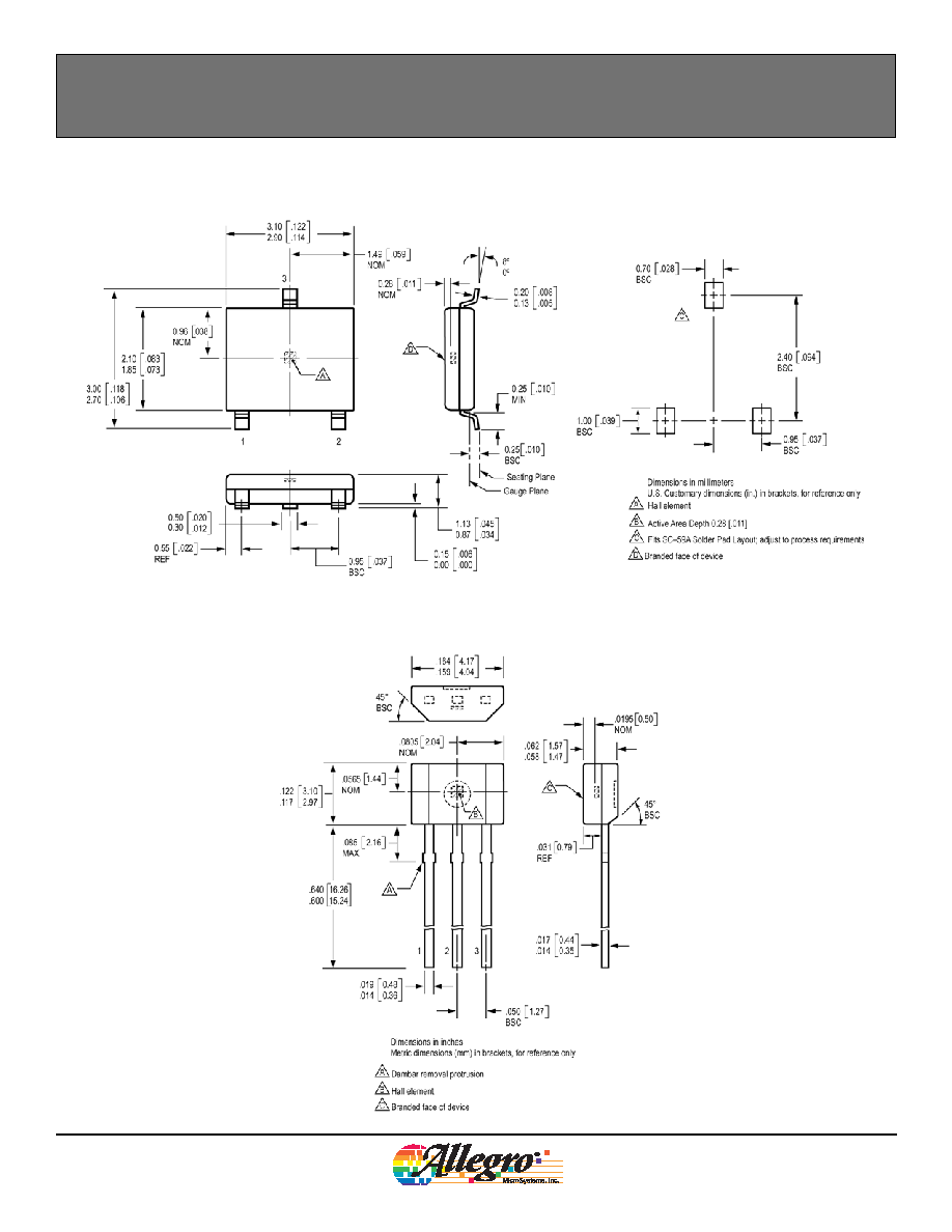
Package LH, 3-Pin (SOT-23W)
Package UA, 3-Pin

12
A3245-DS, Rev. 1
Worcester, Massachusetts 01615-0036 (508) 853-5000
115 Northeast Cutoff, Box 15036
www.allegromicro.com
Allegro MicroSystems, Inc.
Chopper-Stabilized Omnipolar Hall Effect Switches
A3245
The products described herein are manufactured under one
or more of the following U.S. patents: 5,045,920; 5,264,783;
5,442,283; 5,389,889; 5,581,179; 5,517,112; 5,619,137; 5,621,319;
5,650,719; 5,686,894; 5,694,038; 5,729,130; 5,917,320; and other
patents pending.
Allegro MicroSystems, Inc. reserves the right to make, from time
to time, such de par tures from the detail spec i fi ca tions as may be
required to permit improvements in the per for mance, reliability,
or manufacturability of its products. Before placing an order, the
user is cautioned to verify that the information being relied upon is
current.
Allegro products are not authorized for use as critical compo-
nents in life-support devices or sys tems without express written
approval.
The in for ma tion in clud ed herein is believed to be ac cu rate and
reliable. How ev er, Allegro MicroSystems, Inc. assumes no re spon -
si bil i ty for its use; nor for any in fringe ment of patents or other
rights of third parties which may result from its use.
Copyright © 2005 Allegro MicroSystems, Inc.