 | –≠–ª–µ–∫—Ç—Ä–æ–Ω–Ω—ã–π –∫–æ–º–ø–æ–Ω–µ–Ω—Ç: A3251JUA | –°–∫–∞—á–∞—Ç—å:  PDF PDF  ZIP ZIP |
A3250 and A3251
A3250-DS
Worcester, Massachusetts 01615-0036 (508) 853-5000
115 Northeast Cutoff, Box 15036
www.allegromicro.com
Allegro MicroSystems, Inc.
AB SO LUTE MAX I MUM RAT INGS
Supply Voltage, V
CC
......................................26.5 V
Reverse-Supply Voltage, V
RCC
........................≠18 V
Zener Overvoltage, V
Z
.......................................30 V
Output Current, I
OUT
.........................................20 mA
Magnetic Flux Density, B .........................Unlimited
Operating Temperature
Ambient,
T
A
, Range J................. ≠40∫C to 115∫C
Ambient,
T
A
, Range L................ ≠40∫C to 150∫C
Maximum
Junction,
T
J(max)
........................165∫C
Storage Temperature, T
S
.................. ≠65∫C to 170∫C
On-chip protection against:
Supply transients
Output short-circuits
Reverse-battery condition
Field-Programmable, Chopper-Stabilized
Unipolar Hall-Effect Switches
Features and Benefits
The A3250 and A3251 are field-programmable, chopper-stabilized, unipolar Hall-
effect switches designed for use in high-temperature applications. These devices
use a chopper-stabilization technique to eliminate offset inherent in single-element
devices.
The A3250 and A3251 are externally programmable devices. The devices have a
wide range of programmability of the magnetic operate point (B
OP
) while the hys-
teresis remains fixed. This advanced feature allows for optimization of the sensor
switchpoint and can drastically reduce the effects of variations found in a produc-
tion environment, such as magnet and device placement tolerances.
These devices provide on-chip transient protection. A Zener clamp on the power
supply protects against overvoltage conditions on the supply line. These devices
also include short-circuit protection on the output.
The output of the A3250 switches LOW when subjected to a south-polarity mag-
netic field with a flux density that exceeds the threshold for B
OP
, and switches
HIGH when the field drops below the magnetic release point, B
RP
. The output of
the A3251 has the opposite polarity, switching HIGH in a south-polarity magnetic
field that B
OP
, and switching LOW when the field drops below B
RP
.
The other differences in the devices are the power-on state. The A3250 powers-on
in the HIGH state, while the A3251 powers-on in the LOW state.
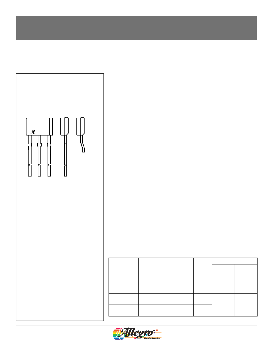
These devices are available in a TO-92 three-lead ultra-mini SIP (Single In-line
Package), with either straight or formed and trimmed lead configuration.
1. VCC
2. GND
3. VOUT
Package UA, 3-pin SIP
Chopper stabilization for stable switchpoints
throughout operating temperature range
Externally programmable operate point
(through VCC pin)
On-board voltage regulator for 4.2 V to 24 V
operation
2
3
1
TL Option
Part Number
Package
T
A
(∫C)
B
hys(typ)
(G)
V
OUT
Power-On Running*
A3250JUA
A3250JUATL
Straight lead
Formed lead
≠40 to 115
18
High
Low
A3250LUA
A3250LUATL
Straight lead
Formed lead
≠40 to 150
13
A3251JUA
A3251JUATL
Straight lead
Formed lead
≠40 to 115
18
Low
High
A3251LUA
A3251LUATL
Straight lead
Formed lead
≠40 to 150
13
*In south polarity magnetic field of sufficient strength.
Use the following complete part numbers when ordering:

2
A3250-DS
Worcester, Massachusetts 01615-0036 (508) 853-5000
115 Northeast Cutoff, Box 15036
www.allegromicro.com
Allegro MicroSystems, Inc.
Field-Programmable, Chopper-Stabilized, Unipolar Hall-Effect Switches
A3250 and A3251
Functional Block Diagram
Current Limit
Amp
Regulator
Program/Lock
Low-Pass
Filter
VCC
GND
Programming
Logic
Offset Adjust
VOUT
Dyna
mic
O
ffse
t
Ca
nce
ll
a
t
i
o
n
Sam
p
le
and
H
old
B
OP
B
RP
B
HYS
V
OUT(off)
V
OUT
V
OUT(on)(sat)
Switch
to
Low
Switch
to
High
B+
V+
Hysteresis of
V
OUT
Switching Due to
B
Hysteresis Curves
A3250
B
OP
B
RP
B
HYS
Switch
to
High
Switch
to
Low
B+
V
OUT(off)
V
OUT
V
OUT(on)(sat)
V+
Hysteresis of
V
OUT
Switching Due to
B
A3251
Output voltage in relation to sensed magnetic flux density in a
south polarity magnetic field of sufficient strength. Transition
through B
OP
must precede transition through B
RP
.
3
A3250-DS
Worcester, Massachusetts 01615-0036 (508) 853-5000
115 Northeast Cutoff, Box 15036
www.allegromicro.com
Allegro MicroSystems, Inc.
Field-Programmable, Chopper-Stabilized, Unipolar Hall-Effect Switches
A3250 and A3251
OPERATING CHARACTERISTICS valid over operating T
A
and V
CC
, unless otherwise specified
Characteristic
Symbol
Test Conditions
Min.
Typ.
Max.
Units
ELECTRICAL CHARACTERISTICS
Supply Voltage
1
V
CC
Running mode
4.2
≠
24
V
Output Saturation Voltage
V
OUT(sat)
I
OUT
= 20 mA; Switch state = ON
≠
175
400
mV
Output Leakage Current
I
OFF
V
OUT
= 24 V; Switch state = OFF
≠
≠
10
µA
Supply Current
I
CC(off)
A3250; B < B
RP
; V
OUT
= HIGH
≠
4.0
7.0
mA
A3251; B > B
OP
; V
OUT
= HIGH
≠
4.0
7.0
mA
I
CC(on)
A3250; B > B
OP
; V
OUT
= LOW
≠
6.0
10.0
mA
A3251; B < B
RP
; V
OUT
= LOW
≠
6.0
10.0
mA
Output Rise Time
t
r
R
LOAD
= 820 , C
LOAD
= 10 pF
≠
≠
5.0
µs
Output Fall Time
t
f
R
LOAD
= 820 , C
LOAD
= 10 pF
≠
≠
5.0
µs
Chopping Frequency
f
C
≠
340
≠
kHz
Power-Up Time
t
on
V
OUT
= HIGH
≠
20
50
µs
Output Current Limit
1,2
I
OUT(lim)
Short-circuit protection
60
90
120
mA
Power-On State
POS
A3250; B < B
RP
, t > t
on
≠
HIGH
≠
mV
A3251; B < B
RP
, t > t
on
≠
LOW
≠
mV
MAGNETIC CHARACTERISTICS
Initial Operate Point
B
OP
≠20
13
50
G
Temperature Drift of B
OP
B
OP
B
OP
500 gauss
≠35
≠
35
G
Hysteresis (B
OP
≠ B
RP
)
B
hys
Package T
A
range = J
5.0
18
35
G
Package T
A
range = L
5.0
13
35
G
PROGRAMMING CHARACTERISTICS
Programmable B
OP
Values
3
B
OP(prog)
50
≠
350
G
Number of Programming Bits
≠
Switchpoint set
≠
6
≠
Bit
Programming lock
≠
1
≠
Bit
Resolution
B
RES
≠
7.0
≠
G
TRANSIENT PROTECTION CHARACTERISTICS
Supply Zener Voltage
V
Z
28
≠
≠
V
Supply Zener Current
I
Z
V
CC
= 28 V
≠
≠
13
mA
Reverse Battery Current
I
RCC
V
RCC
= ≠18 V, T
J
< T
J(max)
≠
≠
≠5.0
mA
1
Do not exceed TJ(max): Additional information on power derating is provided in the applications section.
2
Short-circuit protection is not intended for continuous operation; permanent damage may result.
3
Device can be used below 50 G but is not guaranteed to be a unipolar switch. It is the responsibility of the programmer to verify that the desired
switchpoint has been achieved.
4
A3250-DS
Worcester, Massachusetts 01615-0036 (508) 853-5000
115 Northeast Cutoff, Box 15036
www.allegromicro.com
Allegro MicroSystems, Inc.
Field-Programmable, Chopper-Stabilized, Unipolar Hall-Effect Switches
A3250 and A3251
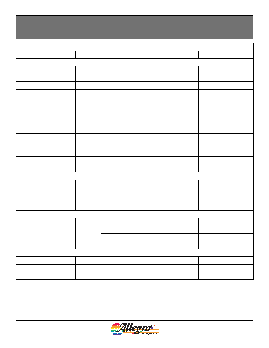
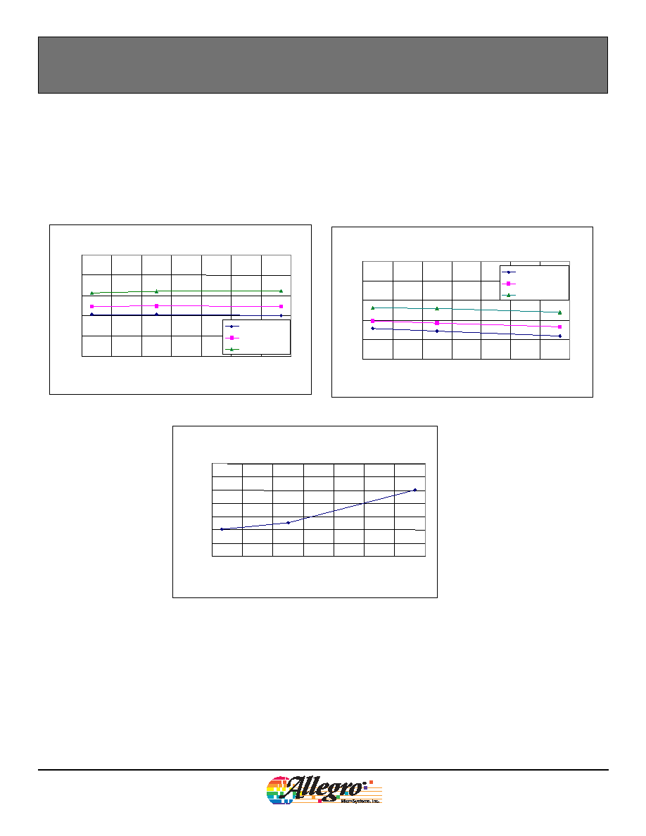
Typical Characterization Data
All data are taken with A3250 devices, the average of 3 lots, 30 pieces per lot
Program Code: 1, V
CC
= 12 V
-5
0
5
10
15
20
25
30
-50
-20
10
40
70
100
130
160
Program Code: 1, V
CC
= 12 V
-20
-15
-10
-5
0
5
10
-50
-20
10
40
70
100
130
160
Program Code: 8, V
CC
= 12 V
40
45
50
55
60
65
70
75
-50
-20
10
40
70
100
130
160
Program Code: 8, V
CC
= 12 V
20
30
40
50
60
-50
-20
10
40
70
100
130
160
Program Code: 16, V
CC
= 12 V
100
105
110
115
120
125
130
-50
-20
10
40
70
100
130
160
Program Code: 16, V
CC
= 12 V
80
85
90
95
100
105
110
-50
-20
10
40
70
100
130
160
Average B
OP
vs. T
A
Average B
OP
vs. T
A
Average B
OP
vs. T
A
Average B
RP
vs. T
A
Average B
RP
vs. T
A
Average B
RP
vs. T
A
T
A
(∞C)
T
A
(∞C)
T
A
(∞C)
T
A
(∞C)
T
A
(∞C)
T
A
(∞C)
Average
B
OP
(G)
Average
B
OP
(G)
Average
B
OP
(G)
Average
B
RP
(G)
Average
B
RP
(G)
Average
B
RP
(G)
5
A3250-DS
Worcester, Massachusetts 01615-0036 (508) 853-5000
115 Northeast Cutoff, Box 15036
www.allegromicro.com
Allegro MicroSystems, Inc.
Field-Programmable, Chopper-Stabilized, Unipolar Hall-Effect Switches
A3250 and A3251
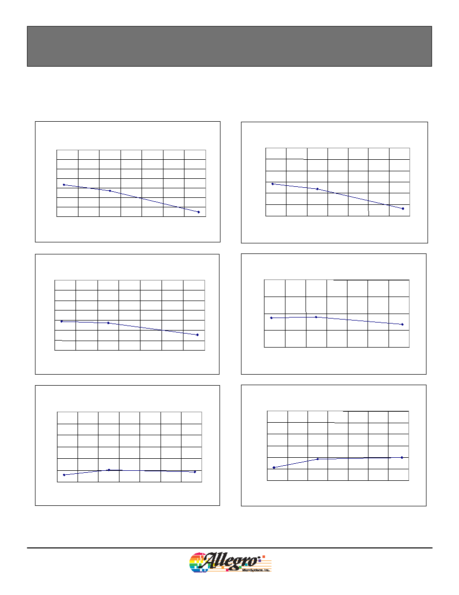
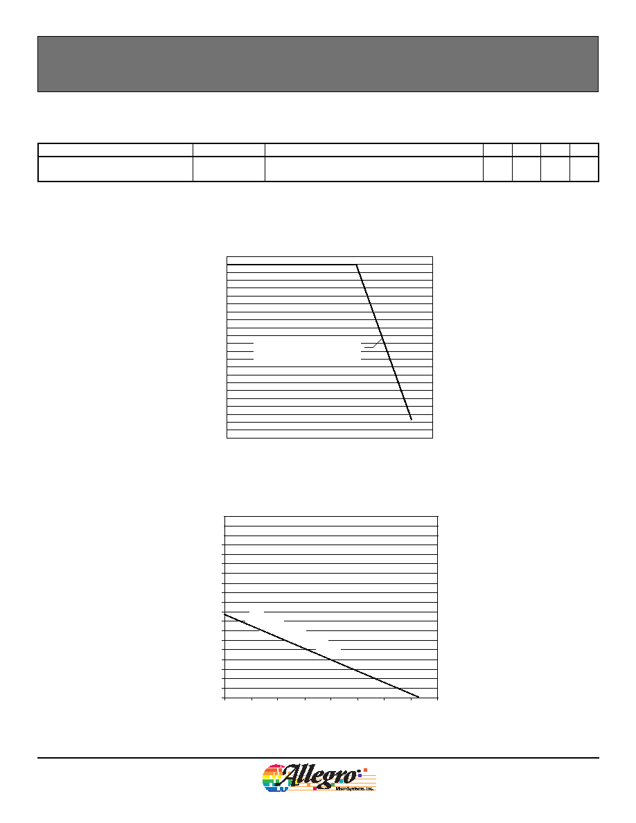
Typical Characterization Data
All data are taken with A3250 devices, the average of 3 lots, 30 pieces per lot
Average B
hys
vs. Temperature
Program Code: 1, V
CC
= 12 V
0
5
10
15
20
25
30
35
-50
-20
10
40
70
100
130
160
Average B
hys
vs. Temperature
Program Code: 16, V
CC
= 12 V
0
5
10
15
20
25
30
35
-50
-20
10
40
70
100
130
160
Average B
hys
vs. Temperature
Program Code: 8, V
CC
= 12 V
0
5
10
15
20
25
30
35
-50
-20
10
40
70
100
130
160
-40∞C to 25∞C and 150∞C to 25∞C
-30
-20
-10
0
10
20
30
Code 1
Code 8
Code 16
-40∞C to 25∞C
150∞C to 25∞C
Average B
OP
vs. Temperature
T
A
(∞C)
T
A
(∞C)
T
A
(∞C)
T
A
(∞C)
Average
B
HYS
(G)
Average
B
HYS
(G)
Average
B
HYS
(G)
Average
B
OP
(G)
6
A3250-DS
Worcester, Massachusetts 01615-0036 (508) 853-5000
115 Northeast Cutoff, Box 15036
www.allegromicro.com
Allegro MicroSystems, Inc.
Field-Programmable, Chopper-Stabilized, Unipolar Hall-Effect Switches
A3250 and A3251
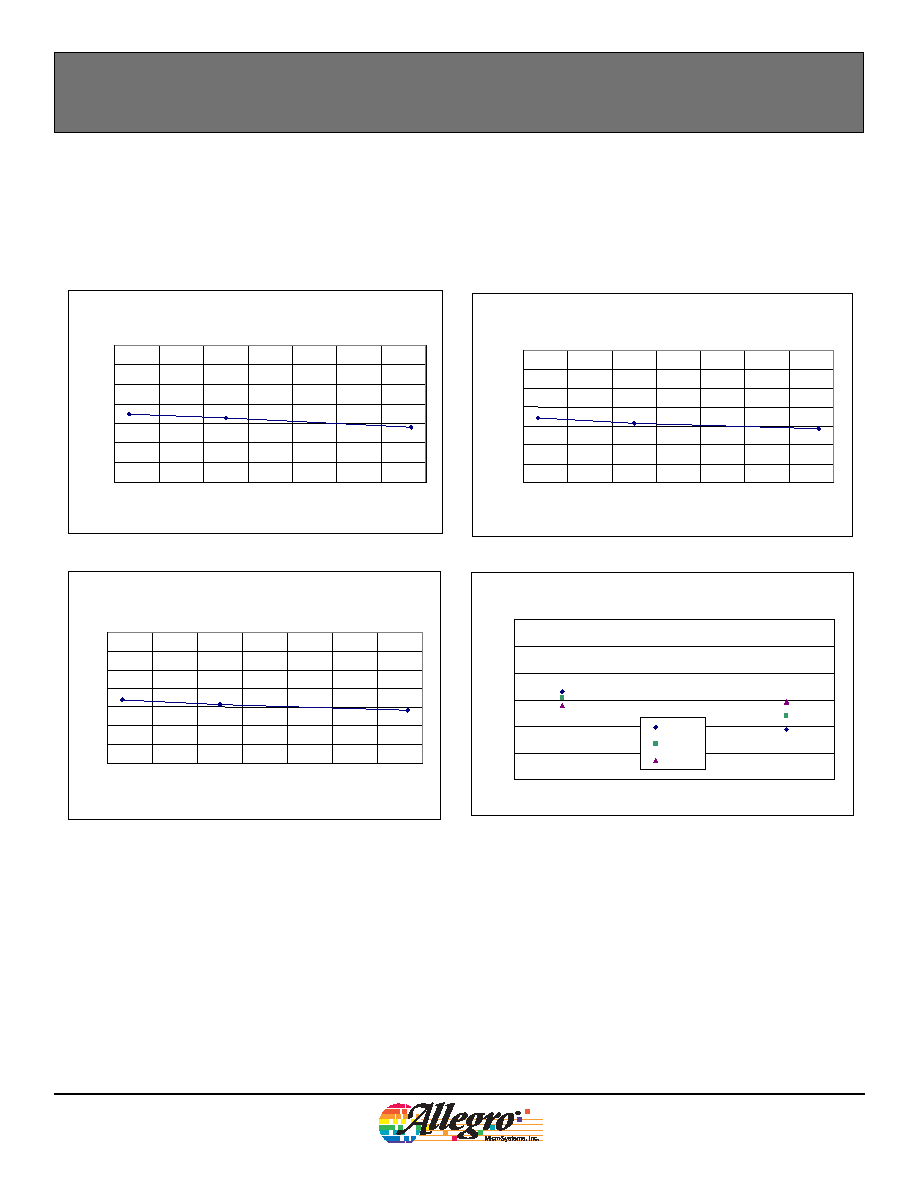
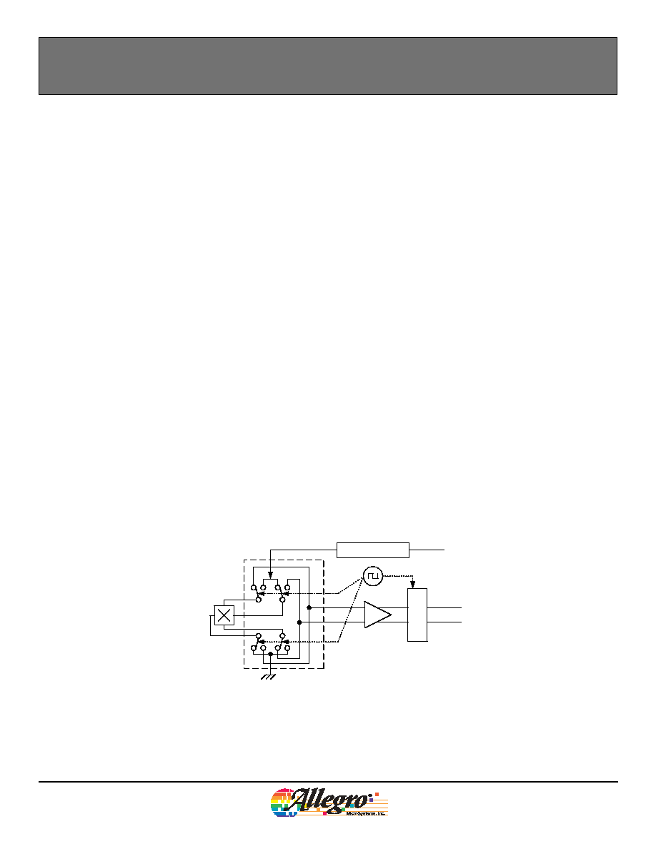
Typical Characterization Data
Average I
CC(on)
vs. Temperature
0
2
4
6
8
10
-50
-20
10
40
70
100
130
160
I
CC
(
on
)
(
mA
)
I
CC(on)
@ 3.8 V
I
CC(on)
@ 12.0 V
I
CC(on)
@ 26.5 V
Average I
CC(off)
vs. Temperature
0
2
4
6
8
10
-50
-20
10
40
70
100
130
160
I
CC
(
off
)
(
mA
)
I
CC(off)
@ 3.8 V
I
CC(off)
@ 12.0 V
I
CC(off)
@ 26.5 V
Average V
OUT(SAT)
vs. Temperature
V
CC
= 3.8 V, I
out
= 20 mA
140
160
180
200
220
240
260
280
-50
-20
10
40
70
100
130
160
V
OUT
(
S
A
T
)
(mV)
T
A
(∞C)
T
A
(∞C)
T
A
(∞C)
All data are taken with A3250 devices, the average of 3 lots, 30 pieces per lot
7
A3250-DS
Worcester, Massachusetts 01615-0036 (508) 853-5000
115 Northeast Cutoff, Box 15036
www.allegromicro.com
Allegro MicroSystems, Inc.
Field-Programmable, Chopper-Stabilized, Unipolar Hall-Effect Switches
A3250 and A3251
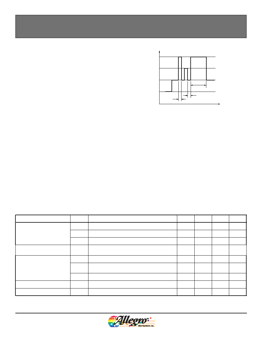
THERMAL CHARACTERISTICS may require derating at maximum conditions, see application information
Characteristic
Symbol
Test Conditions
Min. Typ.
Max Units
Package Thermal Resistance
R
JA
Package UA, minimum-K PCB (single-sided with
copper limited to solder pads)
165
≠
≠
∫C/W
6
7
8
9
2
3
4
5
10
11
12
13
14
15
16
17
18
19
20
21
22
23
24
25
20
40
60
80
100
120
140
160
180
Maximum
Allowable
V
CC
(V)
T
J(max)
= 165∫C; I
CC
= I
CC(max)
Power Derating Curve
(R
JA
= 165 ∫C/W)
Minimum-K PCB, Package UA
V
CC(min)
V
CC(max)
0
100
200
300
400
500
600
700
800
900
1000
1100
1200
1300
1400
1500
1600
1700
1800
1900
20
40
60
80
100
120
140
160
180
Temperature (∞C)
P
o
w
e
r
D
i
s
s
i
pa
ti
on
,
P
D
(m
W)
T
J(max)
= 165∫C; V
CC
= V
CC(max)
; I
CC
= I
CC(max)
Maximum Power Dissipation, P
D(max)
(R
JA
= 165
∫C/W)
Minimum-K
PCB,
Pac
kag
e UA
8
A3250-DS
Worcester, Massachusetts 01615-0036 (508) 853-5000
115 Northeast Cutoff, Box 15036
www.allegromicro.com
Allegro MicroSystems, Inc.
Field-Programmable, Chopper-Stabilized, Unipolar Hall-Effect Switches
A3250 and A3251
Functional Description
Chopper-Stabilized Technique
The Hall sensor is based on a Hall element, a small sheet of
semiconductor material in which a constant bias current flows
when a constant voltage source is applied. The output takes the
form of a voltage measured across the width of the Hall element,
and has negligible value in the absence of a magnetic field.
When a magnetic field is applied with flux lines at right angles
to the current in the Hall element, a small signal voltage directly
proportional to the strength of the magnetic field occurs at the
output of the Hall element.
This small signal voltage is disproportionally small relative to
the offset produced at the input of the device. This makes it very
difficult to process the signal and maintain an accurate, reliable
output over the specified temperature and voltage range. There-
fore, it is important to reduce any distortion of the signal that
could be amplified when the signal is processed.
Chopper stabilization is a unique approach used to minimize
input offset on the Hall IC. This technique removes a key
source of output drift due to temperature and mechanical stress,
and produces a 3X reduction in offset in comparison to other,
conventional methods.
This offset reduction chopping technique is based on a sig-
nal modulation-demodulation process. The undesired offset
signal is separated from the magnetically-induced signal in the
frequency domain. The offset (and any low-frequency noise)
component of the signal can be seen as signal distortion added
after the signal modulation process has taken place. Therefore,
the dc offset is not modulated and remains a low-frequency
component. Consequently, the signal demodulation process acts
as a modulation process for the offset, causing the magnetically-
induced signal to recover its original spectrum at baseband while
the dc offset becomes a high-frequency signal. Then, the signal
passes using a low-pass filter, while the modulated dc offset is
suppressed.
The advantage of this approach is significant offset reduction,
which desensitizes the Hall IC against the effects of temperature
and mechanical stress. The disadvantage is that this technique
features a demodulator that uses a sample-and-hold block to
store and recover the signal. This sampling process can slightly
degrade the SNR (signal-to-noise ratio) by producing replicas of
the noise spectrum at the baseband. This degradation is a function
of the ratio between the white noise spectrum and the sampling
frequency. The effect of the degradation of the SNR is higher
jitter, also known as signal repeatability. However, the jitter in a
continuous-time device can be 5X that of the A3250/A3251.
Chopper stabilization circuit (dynamic quadrature offset cancellation)
Amp
Regulator
Sa
mp
le
an
d
Ho
ld
/
L
PF
9
A3250-DS
Worcester, Massachusetts 01615-0036 (508) 853-5000
115 Northeast Cutoff, Box 15036
www.allegromicro.com
Allegro MicroSystems, Inc.
Field-Programmable, Chopper-Stabilized, Unipolar Hall-Effect Switches
A3250 and A3251
V
PH
V+
t
V
PM
V
PL
0
T
d(1)
T
d(0)
T
d(P)
Figure 1. Pulse amplitudes and durations
PROGRAMMING PROTOCOL CHARACTERISTICS, T
A
= 25∫C, unless otherwise noted
Characteristic
Symbol
Test Conditions
Min.
Typ.
Max.
Units
Programming Voltage
1
V
PL
Minimum voltage range during programming
4.5
5.0
5.5
V
V
PM
10
11
12
V
V
PH
23
25
26
V
Programming Current
2
I
PP
Maximum supply current during programming
≠
500
≠
mA
Pulse Width
t
d(0)
OFF time between programming bits
20
≠
≠
µs
t
d(1)
Pulse duration (ON time) for enable, address, fuse
blowing or lock bits
20
≠
≠
µs
t
d(P)
Pulse duration (ON time) for fuse blowing
100
300
≠
µs
Pulse Rise Time
t
r
V
PL
to V
PM
;
V
PL
to V
PH
11
≠
≠
µs
Pulse Fall Time
t
f
V
PM
to V
PL
; V
PH
to V
PL
5
≠
≠
µs
1
Programming voltages are measured at the VCC pin.
2
A bypass capacitor with a minimum capacitance of 0.1 µF must be connected from VCC to the GND pin of the device in order to provide
the current necessary to blow the fuse.
Additional information on device programming and program-
ming products is available on www. allegromicro.com. Program-
ming hardware is available for purchase, and programming
software is available free of charge.
Programming Protocol
The operate switchpoint, B
OP
, can be field-programmed. To do
so, a coded series of voltage pulses through the VCC pin is used
to set bitfields in onboard registers. The effect on the device
output can be monitored, and the registers can be cleared and
set repeatedly until the required B
OP
is achieved. To make the
setting permanent, bitfield-level solid state fuses are blown, and
finally, a device-level fuse is blown, blocking any further cod-
ing. It is not necessary to program the release switchpoint, B
RP
,
because the difference between B
OP
and B
RP
, referred to as the
hysteresis, B
HYS
, is fixed.
The range of values between B
OP(min)
and B
OP(max)
is scaled to
64 increments. The actual change in magnetic flux (G) repre-
sented by each increment is indicated by B
RES
(see the Operating
Characteristics table; however, testing is the only method for
verifying the resulting B
OP
). For programming, the 64 incre-
ments are individually identified using 6 data bits, which are
physically represented by 6 bitfields in the onboard registers.
By setting these bitfields, the corresponding calibration value is
programmed into the device.
Three voltage levels are used in programming the device: a low
voltage, V
PL
, a minimum required to sustain register settings; a
mid-level voltage, V
PM
, used to increment the address counter
in the device; and a high voltage, V
PH
, used to separate sets of
V
PM
pulses (when short in duration) and to blow fuses (when
long in duration). A fourth voltage level, essentially 0 V, is used
to clear the registers between pulse sequences. The pulse values
are shown in the Programming Protocol Characteristics table and
in figure 1.
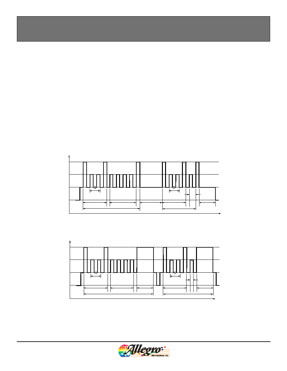
Code Programming.
Each bitfield must be individually set. To
do so, a pulse sequence must be transmitted for each bitfield that
is being set to 1. If more than one bitfield is being set to 1, all
pulse sequences must be sent, one after the other, without allow-
ing V
CC
to fall to zero (which clears the registers).
The same pulse sequence is used to provisionally set bitfields as
is used to permanently set bitfield-level fuses. The only differ-
ence is that when provisionally setting bitfields, no fuse-blowing
pulse is sent at the end of the pulse sequence.
10
A3250-DS
Worcester, Massachusetts 01615-0036 (508) 853-5000
115 Northeast Cutoff, Box 15036
www.allegromicro.com
Allegro MicroSystems, Inc.
Field-Programmable, Chopper-Stabilized, Unipolar Hall-Effect Switches
A3250 and A3251
The pulse sequences consist of the following groups of pulses:
1. An enable sequence.
2. A bitfield address sequence.
3. When permanently setting the bitfield, a long V
PH
fuse-blow-
ing pulse. (Note: Blown bit fuses cannot be reset.) When
provisionally trying a value, a short V
PH
pulse.
4. When permanently setting the bitfield, the level of V
CC
must
be allowed to drop to zero between each pulse sequence, in
order to clear all registers. However, when provisionally set-
ting bitfields, V
CC
must be maintained at V
PL
between pulse
sequences, in order to maintain the prior bitfield settings while
preparing to set additional bitfields.
Bitfields that are not set are evaluated as zeros. The bitfield-level
fuses for 0 value bitfields are never blown. This prevents inad-
vertently setting the bitfield to 1. Instead, blowing the device-
level fuse protects the 0 bitfields from being accidentally set in
the future.
Two pulse sequences for provisionally trying the calibration
value 5 are shown in figure 2. Because the bitfields must be set
individually, 5
10
must be programmed as binary 101. Bit 3 is
set to 1 (000100
2
, which is 4
10
), then bit 1 is set to 1 (000001
2
,
which is 1
10
). Bit 2 is ignored, and so remains 0.
Two pulse sequences for permanently setting the calibration
value 5 are shown in figure 3. The final V
PH
pulse, which was
used as a short delimiter when trying values, is maintained for a
longer period, enough to blow the corresponding bitfield-level
fuse.
V
PH
V+
t
V
PM
V
PL
0
Encode 00100
2
(4
10
)
Enable
7 pulses
7 pulses
Address
Address
Blow
Blow
Enable
Encode 00001
2
(1
10
)
Figure 3. Pulse sequence to permanently encode calibration value 5 (101 binary, or
bitfield address 3 and bitfield address 1).
V
PH
V+
t
V
PM
V
PL
0
Try 00100
2
(4
10
)
Enable
7 pulses
7 pulses
Address
Address
Clear
Enable
Try 00001
2
(1
10
)
Optional
Monitoring
Optional
Monitoring
Figure 2. Pulse sequence to provisionally try calibration value 5 (101 binary, or bitfield
address 3 and bitfield address 1).
11
A3250-DS
Worcester, Massachusetts 01615-0036 (508) 853-5000
115 Northeast Cutoff, Box 15036
www.allegromicro.com
Allegro MicroSystems, Inc.
Field-Programmable, Chopper-Stabilized, Unipolar Hall-Effect Switches
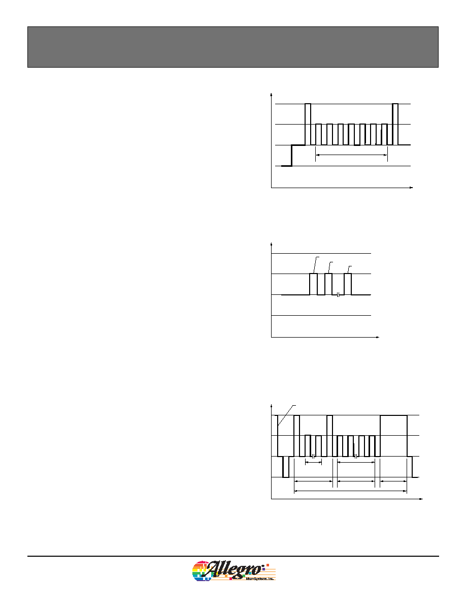
A3250 and A3251
V
PH
V+
t
V
PM
V
PL
0
Address 1
Address 2
Address n (
63)
Figure 5. Pulse sequence to select addresses
Falling edge of final B
OP
address digit
V
PH
V+
t
V
PM
V
PL
0
Encode Lock Bit
Enable
Address
Blow
7 pulses
65 pulses
Figure 6. Pulse sequence to encode lock bit
Lock Bit Programming.
After the desired B
OP
calibration value
is programmed, and all of the corresponding bitfield-level fuses
are blown, the device-level fuse should be blown. To do so, the
lock bit (bitfield address 65) should be encoded as 1 and have
its fuse blown. This is done in the same manner as permanently
setting the other bitfields, as shown in figure 6.
Address Selection.
After addressing mode is enabled, the
target bitfield address, is indicated by a series of VPM pulses,
as shown in figure 3. When provisionally trying a value, this
sequence is followed by a short V
PH
pulse, which serves to
delimit the address and set the corresponding bitfield. When
permanently setting a bitfield, the V
PH
pulse is continued for a
longer period of time, suffienct to not only set the bitfield to 1,
but also to blow the bitfield fuse.
Enabling Addressing Mode.
The first segment of code is a
keying sequence used to enable the bitfield addressing mode. As
shown in figure 4, this segment consists of one short V
PH
pulse,
seven or more V
PM
pulses, and one V
PH
pulse, with no supply
interruptions. This sequence is designed to prevent the device
from being programmed accidentally, such as by noise on the
supply line.
V
PH
V+
t
V
PM
V
PL
0
Minimum 7 pulses
Figure 4. Addressing mode enable pulse sequence
12
A3250-DS
Worcester, Massachusetts 01615-0036 (508) 853-5000
115 Northeast Cutoff, Box 15036
www.allegromicro.com
Allegro MicroSystems, Inc.
Field-Programmable, Chopper-Stabilized, Unipolar Hall-Effect Switches
A3250 and A3251
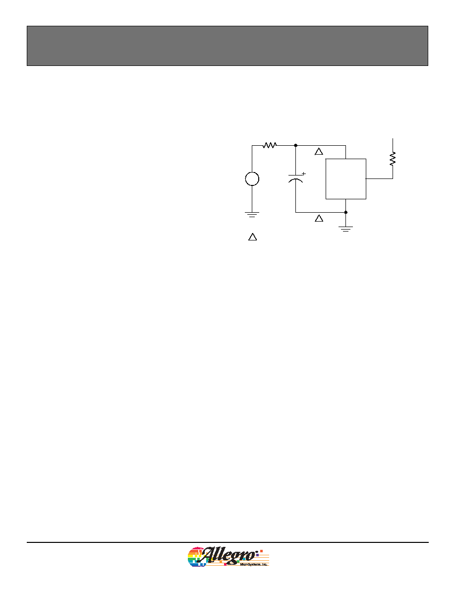
Application Information
For additional general application information, visit the Allegro
MicroSystems Web site at www. allegromicro.com.
Typical application circuit
Typical Application Circuit
It is strongly recommended that an external ceramic bypass
capacitor, C
BYP
, in the range of 0.01 µF to 0.1 µF be connected
between the VCC pin and the supply and GND pin to reduce
both external noise and noise generated by the chopper-stabiliza-
tion technique. (The diagram at the right shows C
BYP
at 0.1 µF.)
C
BYP
should be installed so that the traces that connect it to the
A3250/A3251 are no greater than 5 mm in length.
The series resistor R
S
, in combination with C
BYP
creates a filter
for EMI pulses. (Additional information on EMC is provided
on the Allegro MicroSystems Web site.) R
S
will have a drop
of approximately 800 mV. This must be taken into consider-
ation when determining the minimum VCC requirement for the
A3250/A3251. The pull-up resistor, R
L
, should be chosen to
limit the current through the output transistor; do not exceed the
maximum continuous output current of the device.
GND
A3250/A3251
VCC
V
Supply
0.1
µF
A
R
L
C
BYP
R
S
100
1.2 k
5V
VOUT
A
A
Maximum separation 5 mm
from C
BYP
to device

13
A3250-DS
Worcester, Massachusetts 01615-0036 (508) 853-5000
115 Northeast Cutoff, Box 15036
www.allegromicro.com
Allegro MicroSystems, Inc.
Field-Programmable, Chopper-Stabilized, Unipolar Hall-Effect Switches
A3250 and A3251
Power Derating
The device must be operated below the maximum junction
temperature of the device, T
J(max)
. Under certain combinations of
peak conditions, reliable operation may require derating sup-
plied power or improving the heat dissipation properties of the
application. This section presents a procedure for correlating
factors affecting operating T
J
. (Thermal data is also available on
the Allegro MicroSystems Web site.)
The Package Thermal Resistance, R
JA
, is a figure of merit sum-
marizing the ability of the application and the device to dissipate
heat from the junction (die), through all paths to the ambient air.
Its primary component is the Effective Thermal Conductivity,
K, of the printed circuit board, including adjacent devices and
traces. Radiation from the die through the device case, R
JC
, is
relatively small component of R
JA
. Ambient air temperature,
T
A
, and air motion are significant external factors, damped by
overmolding.
The effect of varying power levels (Power Dissipation, P
D
), can
be estimated. The following formulas represent the fundamental
relationships used to estimate T
J
, at P
D
.
P
D
= V
IN
◊
I
IN
(1)
T = P
D
◊
R
JA
(2)
T
J
= T
A
+ T
(3)
For example, given common conditions such as: T
A
= 25∞C,
V
CC
= 12 V, I
CC
= 4 mA, and R
JA
= 165 ∞C/W, then:
P
D
= V
CC
◊
I
CC
= 12 V
◊
4 mA = 48 mW
T = P
D
◊
R
JA
= 48 mW
◊
165 ∞C/W = 8∞C
T
J
= T
A
+
T = 25∞C + 8∞C = 33∞C
A worst-case estimate, P
D(max)
, represents the maximum allow-
able power level (V
CC(max)
, I
CC(max)
), without exceeding T
J(max)
,
at a selected R
JA
and T
A
.
Example: Reliability for V
CC
at T
A
=
150∞C, package UA, using
minimum-K PCB.
Observe the worst-case ratings for the device, specifically:
R
JA
=
165∞C/W, T
J(max)
=
165∞C, V
CC(max)
=
24 V, and
I
CC(max)
=
10
mA.
Calculate the maximum allowable power level, P
D(max)
. First,
invert equation 3:
T
max
= T
J(max)
≠ T
A
= 165
∞C
≠
150
∞C = 15
∞C
This provides the allowable increase to T
J
resulting from internal
power dissipation. Then, invert equation 2:
P
D(max)
=
T
max
˜ R
JA
= 15∞C ˜ 165 ∞C/W = 91 mW
Finally, invert equation 1 with respect to voltage:
V
CC(est)
= P
D(max)
˜ I
CC(max)
= 91 mW ˜ 10 mA = 9 V
The result indicates that, at T
A
, the application and device can
dissipate adequate amounts of heat at voltages V
CC(est)
.
Compare V
CC(est)
to V
CC(max)
. If V
CC(est)
V
CC(max)
, then reli-
able operation between V
CC(est)
and V
CC(max)
requires enhanced
R
JA
. If V
CC(est)
V
CC(max)
, then operation between V
CC(est)
and
V
CC(max)
is reliable under these conditions.
14
A3250-DS
Worcester, Massachusetts 01615-0036 (508) 853-5000
115 Northeast Cutoff, Box 15036
www.allegromicro.com
Allegro MicroSystems, Inc.
Field-Programmable, Chopper-Stabilized, Unipolar Hall-Effect Switches
A3250 and A3251
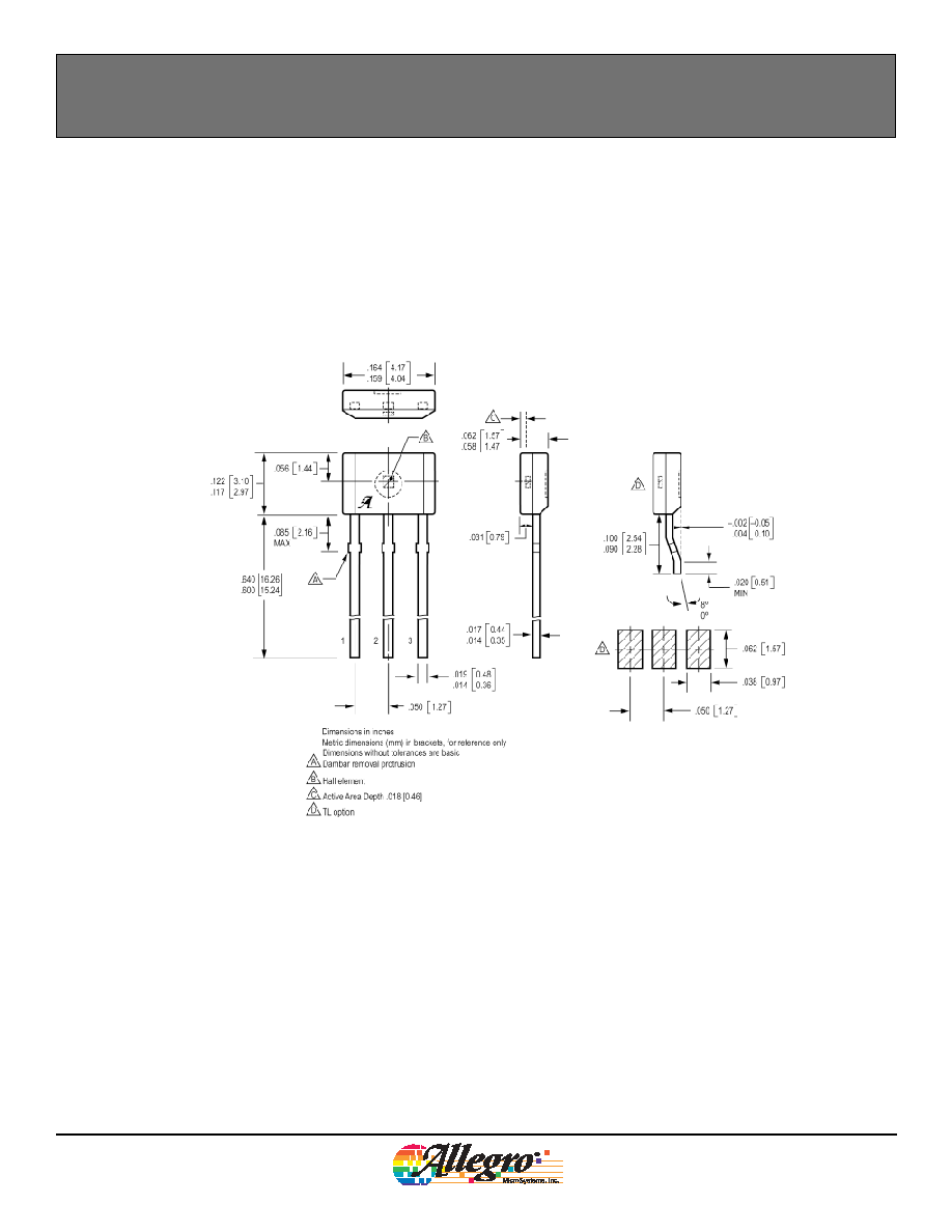
Package UA, 3-Pin; (TO-92)
The products described herein are manufactured under one or more of the following U.S. patents: 5,045,920;
5,264,783; 5,442,283; 5,389,889; 5,581,179; 5,517,112; 5,619,137; 5,621,319; 5,650,719; 5,686,894; 5,694,038;
5,729,130; 5,917,320; and other patents pending.
Allegro MicroSystems, Inc. reserves the right to make, from time to time, such de par tures from the detail spec-
i fi ca tions as may be required to permit improvements in the per for mance, reliability, or manufacturability of its
products. Before placing an order, the user is cautioned to verify that the information being relied upon is current.
Allegro products are not authorized for use as critical components in life-support devices or sys tems without
express written approval.
The in for ma tion in clud ed herein is believed to be ac cu rate and reliable. How ev er, Allegro MicroSystems, Inc.
assumes no re spon si bil i ty for its use; nor for any in fringe ment of patents or other rights of third parties which may
result from its use.
Copyright © 2004 Allegro MicroSystems, Inc.

15
A3250-DS
Worcester, Massachusetts 01615-0036 (508) 853-5000
115 Northeast Cutoff, Box 15036
www.allegromicro.com
Allegro MicroSystems, Inc.
Field-Programmable, Chopper-Stabilized, Unipolar Hall-Effect Switches
A3250 and A3251