 | –≠–ª–µ–∫—Ç—Ä–æ–Ω–Ω—ã–π –∫–æ–º–ø–æ–Ω–µ–Ω—Ç: A3425EL-T | –°–∫–∞—á–∞—Ç—å:  PDF PDF  ZIP ZIP |

A3425
A3425DS-Rev. !
Worcester, Massachusetts 01615-0036 (508) 853-5000
115 Northeast Cutoff, Box 15036
www.allegromicro.com
Allegro MicroSystems, Inc.
AB SO LUTE MAX I MUM RAT INGS
Supply Voltage, V
CC
.......................................26.5 V
Reverse-Battery Voltage, V
RCC
........................≠18 V
Output Off Voltage, V
OUTPUT
..............................V
CC
Output Sink Current, I
OUTPUT(SINK)
. Internally Limited
Magnetic Flux Density, B .......................... Unlimited
Operating Temperature
Ambient,
T
A
, Range E.................. ≠40∫C to 85∫C
Range L................ ≠40∫C to 150∫C
Maximum
Junction,
T
J(max)
........................165∫C
Storage Temperature, T
S
.................. ≠65∫C to 170∫C
∑
Two matched Hall effect switches on a single substrate
∑ Sensor element spacing approximately 1 mm
∑ Superior temperature stability
∑ 3.3 V to 18 V operation
∑ Integrated ESD diode from OUTPUT and VCC pins to GND
∑ High-sensitivity
switchpoints
∑ Robust structure for EMC protection
∑ Solid-state
reliability
The A3425 is a dual-output channel, bipolar switch with two separate Hall-effect
sensor circuits, each providing a separate digital output for speed and direction
signal processing capability. Each sensor circuit has its own independent Hall
element, which are photolithographically aligned to better than 1 µm. Maintaining
accurate mechanical location between the two active Hall elements eliminates the
major manufacturing hurdle encountered in fi ne-pitch detection applications. The
A3425 is a highly sensitive, temperature-stable magnetic sensing device, which
is ideal for use in ring magnet-based speed and direction systems used in harsh
automotive and industrial environments.
The A3425 monolithic integrated circuit contains two independent Hall effect
switches, located approximately 1 mm apart. The digital outputs are 90∫ out of
phase so that the outputs are in quadrature with the proper ring magnet design.
This allows for easy processing of speed and direction signals. Extremely low-
drift amplifi ers guarantee symmetry between the switches to maintain signal
quadrature. The patented chopper stabilization technique cancels offsets in
each channel, and provides stable operation over the operating temperature and
voltage ranges. An on-chip regulator allows the use of this device over a wide
operating voltage range. Post-assembly factory programming provides sensitive
switchpoints that are symmetrical between the two switches.
The A3425 is available in a plastic 8-pin SOIC surface mount package and a plas-
tic 4-pin SIP, both in two temperature ranges. Each package is available in a lead
(Pb) free version with 100% matte tin plated leadframe.
Ultra-Sensitive Dual-Channel Quadrature Hall-Effect Bipolar Switch
1
2
3
4
8
7
6
5
VCC
OUTPUTA
OUTPUTB
GND
No connection
No connection
No connection
No connection
Package L, 8-pin SOIC
Package K, 4-pin SIP
1 2 3 4
1. VCC
2. OUTPUTA
3. OUTPUTB
4. GND
Features and Benefi ts

2
A3425DS-Rev. !
Worcester, Massachusetts 01615-0036 (508) 853-5000
115 Northeast Cutoff, Box 15036
www.allegromicro.com
Allegro MicroSystems, Inc.
Ultra-Sensitive Dual-Channel Quadrature Hall-Effect Bipolar Switch
A3425
Amp
Output
Drive
Amp
Output
Drive
4 Bits
4 Bits
Regulator
Programmable
Trim
OUTPUTA
OUTPUTB
VCC
8 Bits
Sam
p
le
and
H
old
Dyna
mic
O
ffse
t
Ca
nce
l
l
a
ti
on
Sam
p
le
and
H
old
Dyna
mic
O
ffse
t
Ca
nce
l
l
a
ti
on
Pass
Filter
Low-
Pass
Filter
Low-
GND
Functional Block Diagram
Terminal List
Symbol
Description
Package
K
L
VCC
Connects power supply to on-chip voltage regulator
1
1
OUTPUTA
Output from fi rst Schmitt circuit
2
2
OUTPUTB
Output from second Schmitt circuit
3
3
GND
Ground
4
4
≠
No connection
≠
5, 6, 7, 8
3
A3425DS-Rev. !
Worcester, Massachusetts 01615-0036 (508) 853-5000
115 Northeast Cutoff, Box 15036
www.allegromicro.com
Allegro MicroSystems, Inc.
Ultra-Sensitive Dual-Channel Quadrature Hall-Effect Bipolar Switch
A3425
*Contact Allegro for additional packing options.
Part Number
Pb-free
Packing*
Mounting
Ambient, T
A
A3425EK
≠
Bulk, 98 pieces/bag
4-pin SIP through hole
≠40∫C to 85∫C
A3425EK-T
Yes
Bulk, 98 pieces/bag
A3425EKTN
≠
13-in. reel, 4000 pieces/reel
A3425EKTN-T
Yes
13-in. reel, 4000 pieces/reel
A3425EL
≠
Bulk, 500 pieces/bag
8-pin SOIC surface mount
A3425EL-T
Yes
Bulk, 500 pieces/bag
A3425ELTR
≠
13-in. reel, 3000 pieces/reel
A3425ELTR-T
Yes
13-in. reel, 3000 pieces/reel
A3425LK
≠
Bulk, 98 pieces/bag
4-pin SIP through hole
≠40∫C to 150∫C
A3425LK-T
Yes
Bulk, 98 pieces/bag
A3425LKTN
≠
13-in. reel, 4000 pieces/reel
A3425LKTN-T
Yes
13-in. reel, 4000 pieces/reel
A3425LL
≠
Bulk, 500 pieces/bag
8-pin SOIC surface mount
A3425LL-T
Yes
Bulk, 500 pieces/bag
A3425LLTR
≠
13-in. reel, 3000 pieces/reel
A3425LLTR-T
Yes
13-in. reel, 3000 pieces/reel
Product Selection Guide

4
A3425DS-Rev. !
Worcester, Massachusetts 01615-0036 (508) 853-5000
115 Northeast Cutoff, Box 15036
www.allegromicro.com
Allegro MicroSystems, Inc.
Ultra-Sensitive Dual-Channel Quadrature Hall-Effect Bipolar Switch
A3425
OPERATING CHARACTERISTICS
Valid over operating temperature ranges unless otherwise noted; typical data applies to
V
CC
= 12 V, and T
A
= 25∫C
Characteristic
Symbol
Test Conditions
Min. Typ. Max
Units
ELECTRICAL CHARACTERISTICS
Supply Voltage
1
V
CC
Operating; T
A
150∞C
3.3
≠
18
V
Output Leakage Current
I
OUTPUT(OFF)
Either output
≠
< 1
10
µA
Output Rise Time
t
r
C
LOAD
= 20 pF, R
LOAD
= 820
≠
110
≠
ns
Output Fall Time
t
f
C
LOAD
= 20 pF, R
LOAD
= 820
≠
55
≠
ns
Supply Current
I
CC(OFF)
B < B
RP(A)
,B < B
RP(B)
≠
3.5
6.0
mA
I
CC(ON)
B > B
OP(A)
,B > B
OP(B)
≠
4.0
6.0
mA
Low Output Voltage
V
OUTPUT(ON)
Both outputs; I
OUTPUT(SINK)
= 20 mA; B > B
OP(A)
,
B > B
OP(B)
≠
160
500
mV
Output Sink Current
I
OUTPUT(SINK)
≠
≠
20
mA
Output Sink Current, Continuous
2
I
OUTPUT(SINK)C
T
J
< T
J(max)
,V
OUTPUT
= 12 V
≠
≠
70
mA
Output Sink Current, Peak
3
I
OUTPUT(SINK)P
t < 3 seconds
≠
≠
220
mA
Chopping Frequency
f
C
≠
340
≠
kHz
TRANSIENT PROTECTION CHARACTERISTICS
Supply Zener Voltage
V
Z
I
CC
= 15 mA
28
33
37
V
Supply Zener Current
4
I
Z
V
S
= 28 V
≠
≠
9.0
mA
Reverse-Battery Current
I
RCC
V
RCC
= ≠18 V, T
J
< T
J(max)
≠
2
15
mA
Continued on the next page...
5
A3425DS-Rev. !
Worcester, Massachusetts 01615-0036 (508) 853-5000
115 Northeast Cutoff, Box 15036
www.allegromicro.com
Allegro MicroSystems, Inc.
Ultra-Sensitive Dual-Channel Quadrature Hall-Effect Bipolar Switch
A3425
MAGNETIC CHARACTERISTICS, K Package
5
Operate Point: B > B
OP
B
OP(A)
, B
OP(B)
≠
7
35
G
Release Point: B < B
RP
B
RP(A)
, B
RP(B)
≠35
≠7
≠
G
Hysteresis: B
OP(A)
≠ B
RP(A)
,
B
OP(B)
≠ B
RP(B)
B
HYS(A)
, B
HYS(B)
5
16
40
G
Symmetry: Channel A, Channel B,
B
OP(A)
+ B
RP(A)
,
B
OP(B)
+ B
RP(B)
SYM
A
, SYM
B
≠40
≠
40
G
Operate Symmetry: B
OP(A)
≠ B
OP(B)
SYM
AB(OP)
≠30
≠
30
G
Release Symmetry: B
RP(A)
≠ B
RP(B)
SYM
AB(RP)
≠30
≠
30
G
MAGNETIC CHARACTERISTICS, L Package
5
Operate Point: B > B
OP
B
OP(A)
, B
OP(B)
≠
7
30
G
Release Point: B < B
RP
B
RP(A)
, B
RP(B)
≠30
≠7
≠
G
Hysteresis: B
OP(A)
≠ B
RP(A)
,
B
OP(B)
≠ B
RP(B)
B
HYS(A)
, B
HYS(B)
5
14
35
G
Symmetry: Channel A, Channel B,
B
OP(A)
+ B
RP(A)
,
B
OP(B)
+ B
RP(B)
SYM
A
, SYM
B
≠35
≠
35
G
Operate Symmetry: B
OP(A)
≠ B
OP(B)
SYM
AB(OP)
≠25
≠
25
G
Release Symmetry: B
RP(A)
≠ B
RP(B)
SYM
AB(RP)
≠25
≠
25
G
1
When operating at maximum voltage, never exceed maximum junction temperature, T
J(max)
. Refer to power derating curve charts.
2
Device will survive the current level specifi ed, but operation within magnetic specifi cation cannot be guaranteed.
3
Short circuit of the output to VCC is protected for the time duration specifi ed.
4
Maximum specifi cation limit is equivalent to I
CC(max)
+ 3 mA.
5
Magnetic fl ux density, B, is indicated as a negative value for north-polarity magnetic fi elds, and as a positive value for south-polarity
magnetic fi elds. This so-called algebraic convention supports arithmetic comparison of north and south polarity values, where the
relative strength of the fi eld is indicated by the absolute value of B, and the sign indicates the polarity of the fi eld (for example, a ≠100
G fi eld and a 100 G fi eld have equivalent strength, but opposite polarity).
OPERATING CHARACTERISTICS (continued)
Valid over operating temperature ranges unless otherwise noted; typical
data applies to V
CC
= 12 V, and T
A
= 25∫C
Characteristic
Symbol
Test Conditions
Min. Typ. Max
Units
EMC
Contact Allegro MicroSystems for EMC performance.

6
A3425DS-Rev. !
Worcester, Massachusetts 01615-0036 (508) 853-5000
115 Northeast Cutoff, Box 15036
www.allegromicro.com
Allegro MicroSystems, Inc.
Ultra-Sensitive Dual-Channel Quadrature Hall-Effect Bipolar Switch
A3425
THERMAL CHARACTERISTICS may require derating at maximum conditions, see application information
Characteristic
Symbol
Test Conditions
Value Units
Package Thermal Resistance
R
JA
Package K, minimum-K PCB (single-sided with copper limited to
solder pads)
177
∫C/W
Package L, minimum-K PCB (single-sided with copper limited to
solder pads)
140
∫C/W
Package L, high-K PCB (multilayer with signifi cant copper
areas, based on JEDEC standard)
80
∫C/W
6
7
8
9
2
3
4
5
10
11
12
13
14
15
16
17
18
19
20
20
40
60
80
100
120
180
140
160
Temperature (∫C)
Maximum
Allowable
V
CC
(V)
T
J(max)
= 165∫C; I
CC
= I
CC(max)
Power Derating Curve
(R
JA
= 140 ∫C/W)
Minimum-K PCB, Package L
(R
JA
= 177 ∫C/W)
Minimum-K PCB, Package K
(R
JA
= 80 ∫C/W)
High-K PCB, Package L
V
CC(min)
V
CC(max)
0
100
200
300
400
500
600
700
800
900
1000
1100
1200
1300
1400
1500
1600
1700
1800
1900
20
40
60
80
100
120
140
160
180
Temperature, TA (∞C)
P
o
w
e
r
D
i
s
s
i
pa
ti
on
,
P
D
(m
W)
Power Dissipation versus Temperature
(R
JA
= 140
∫C/W)
Minimum-K
PCB,
Package
L
(R
JA
= 177
∫C/W)
Minimum-K
PCB,
Packa
ge K
(R
JA
=
80
∫C/W)
High
-K
PCB,
Packa
ge
L

7
A3425DS-Rev. !
Worcester, Massachusetts 01615-0036 (508) 853-5000
115 Northeast Cutoff, Box 15036
www.allegromicro.com
Allegro MicroSystems, Inc.
Ultra-Sensitive Dual-Channel Quadrature Hall-Effect Bipolar Switch
A3425
Functional Description
Chopper-Stabilized Technique
When using Hall effect technology, a limiting factor
for switchpoint accuracy is the small signal voltage
developed across the Hall element. This voltage is
disproportionally small relative to the offset that can
be produced at the output of the Hall device. This
makes it diffi cult to process the signal and maintain
an accurate, reliable output over the specifi ed tem-
perature and voltage range.
Chopper stabilization is a unique approach used
to minimize Hall offset on the chip. The patented
Allegro technique, dynamic quadrature offset can-
cellation, removes key sources of the output drift
induced by thermal and mechanical stress. This offset
reduction technique is based on a signal modulation-
demodulation process. The undesired offset signal is
separated from the magnetically induced signal in the
frequency domain through modulation. The subse-
quent demodulation acts as a modulation process for
the offset, causing the magnetically-induced signal to
recover its original spectrum at the baseband level,
while the dc offset becomes a high-frequency signal.
Then, using a low-pass fi lter, the signal passes while
the modulated dc offset is suppressed.
The chopper stabilization technique uses a 170 kHz
high-frequency clock. The Hall element chopping
occurs on each clock edge, resulting in a 340 kHz
chop frequency. This high-frequency operation allows
for a greater sampling rate, which produces higher
accuracy and faster signal processing capability. This
approach desensitizes the chip to the effects of ther-
mal and mechanical stress. The disadvantage to this
approach is that jitter, also known as 360∞ repeatability,
can be induced on the output signal. The sample-and-
hold process, used by the demodulator to store and
recover the signal, can slightly degrade the signal-to-
noise ratio. This is because the process generates rep-
licas of the noise spectrum at the baseband, causing a
decrease in jitter performance. However, the improve-
ment in switchpoint performance, resulting from the
reduction of the effects of thermal and mechanical
stress, outweighs the degradation in the signal-to-noise
ratio.
This technique produces devices that have an
extremely stable quiescent Hall element output volt-
age, are immune to thermal stress, and have precise
recoverability after temperature cycling. This tech-
nique is made possible through the use of a BiCMOS
process, which allows the use of low-offset and
low-noise amplifi ers in combination with high-density
logic integration and sample-and-hold circuits. This
process is illustrated in the following diagram.
Chopper stabilization circuit (dynamic quadrature offset cancellation)
Amp
Regulator
Low-
Pass
Filter
Sa
mp
le
an
d
H
ol
d

8
A3425DS-Rev. !
Worcester, Massachusetts 01615-0036 (508) 853-5000
115 Northeast Cutoff, Box 15036
www.allegromicro.com
Allegro MicroSystems, Inc.
Ultra-Sensitive Dual-Channel Quadrature Hall-Effect Bipolar Switch
A3425
Typical Applications Operation
Quadrature output signal confi guration. The outputs of the two output
channels have a phase difference of 90∫ when used with a properly
designed magnet that has an optimal pole pitch of twice the Hall ele-
ment spacing of 1.0 mm.
B
OP
B
RP
B
HYS
V
OUTPUT(OFF)
V
OUTPUT
V
OUTPUT(ON)(sat)
Switch to Low
Switch to High
B+
V+
Output voltage in relation to sensed magnetic fl ux density. Output on
each channel independently follows the same pattern of transition
through B
OP
followed by transition through B
RP
.
Output Sensor B
Output Sensor A
M agnetic Fie ld
Sensor A
M agnetic Fie ld
Sensor B

9
A3425DS-Rev. !
Worcester, Massachusetts 01615-0036 (508) 853-5000
115 Northeast Cutoff, Box 15036
www.allegromicro.com
Allegro MicroSystems, Inc.
Ultra-Sensitive Dual-Channel Quadrature Hall-Effect Bipolar Switch
A3425
Regulated supply
1
A3425
2
3
4
V
Supply
0.1 uF
V
OUTPUTB
V
OUTPUTA
OUTPUTA
OUTPUTB
GND
VCC
0.1 uF
100
1
A3425
2
3
4
V
Supply
V
OUTPUTB
V
OUTPUTA
OUTPUTA
OUTPUTB
GND
VCC
This device requires minimal protection circuitry
during operation with a low-voltage regulated line.
The on-chip voltage regulator provides immunity
to power supply variations between 3.3 and 18 V.
Because the device has open-collector outputs, pull-
up resistors must be included.
If protection against coupled and injected noise is
required, then a simple low-pass fi lter on the supply
(RC) and a fi ltering capacitor on each of the outputs
may also be needed, as shown in the unregulated
supply diagram.
For applications in which the device receives its
power from unregulated sources, such as a car bat-
tery, full protection is generally required to protect the
device against supply-side transients. Specifi cations
for such transients vary for each application, so the
design of the protection circuit should be optimized
for each application.
For example, the circuit shown in the unregulated
supply diagram includes a Zener diode that offers
high voltage load-dump protection and noise fi ltering
by means of a series resistor and capacitor. In addi-
tion, it includes a series diode that protects against
high-voltage reverse battery conditions.
Unregulated supply
Typical Applications Circuits

10
A3425DS-Rev. !
Worcester, Massachusetts 01615-0036 (508) 853-5000
115 Northeast Cutoff, Box 15036
www.allegromicro.com
Allegro MicroSystems, Inc.
Ultra-Sensitive Dual-Channel Quadrature Hall-Effect Bipolar Switch
A3425
Typical Thermal Performance
The device must be operated below the maximum junction
temperature of the device, T
J(max)
. Under certain combinations of
peak conditions, reliable operation may require derating sup-
plied power or improving the heat dissipation properties of the
application. This section presents a procedure for correlating
factors affecting operating T
J
. (Thermal data is also available on
the Allegro MicroSystems Web site.)
The Package Thermal Resistance, R
JA
, is a fi gure of merit sum-
marizing the ability of the application and the device to dissipate
heat from the junction (die), through all paths to the ambient air.
Its primary component is the Effective Thermal Conductivity,
K, of the printed circuit board, including adjacent devices and
traces. Radiation from the die through the device case, R
JC
, is
relatively small component of R
JA
. Ambient air temperature,
T
A
, and air motion are signifi cant external factors, damped by
overmolding.
The effect of varying power levels (Power Dissipation, P
D
), can
be estimated. The following formulas represent the fundamental
relationships used to estimate T
J
, at P
D
.
P
D
= V
IN
◊
I
IN
(1)
T = P
D
◊
R
JA
(2)
T
J
= T
A
+ T
(3)
For example, given common conditions such as: T
A
= 25∞C,
V
CC
= 12 V, I
CC
= 4 mA, and R
JA
= 140 ∞C/W, then:
P
D
= V
CC
◊
I
CC
= 12 V
◊
4 mA = 48 mW
T = P
D
◊
R
JA
= 48 mW
◊
140 ∞C/W = 7∞C
T
J
= T
A
+
T = 25∞C + 7∞C = 32∞C
A worst-case estimate, P
D(max)
, represents the maximum allow-
able power level (V
CC(max)
, I
CC(max)
), without exceeding T
J(max)
,
at a selected R
JA
and T
A
.
Example: Reliability for V
CC
at T
A
=
150∞C, package L, using
minimum-K PCB
Observe the worst-case ratings for the device, specifi cally:
R
JA
=
140
∞C/W, T
J(max)
=
165∞C, V
CC(max)
=
18
V, and
I
CC(max)
=
6
mA.
Calculate the maximum allowable power level, P
D(max)
. First,
invert equation 3:
T
max
= T
J(max)
≠ T
A
= 165
∞C
≠
150
∞C = 15
∞C
This provides the allowable increase to T
J
resulting from internal
power dissipation. Then, invert equation 2:
P
D(max)
=
T
max
˜ R
JA
= 15∞C ˜ 140 ∞C/W = 107 mW
Finally, invert equation 1 with respect to voltage:
V
CC(est)
= P
D(max)
˜ I
CC(max)
= 107 mW ˜ 6 mA = 18 V
The result indicates that, at T
A
, the application and device can
dissipate adequate amounts of heat at voltages V
CC(est)
.
Compare V
CC(est)
to V
CC(max)
. If V
CC(est)
V
CC(max)
, then reli-
able operation between V
CC(est)
and V
CC(max)
requires enhanced
R
JA
. If V
CC(est)
V
CC(max)
, then operation between V
CC(est)
and
V
CC(max)
is reliable under these conditions.
11
A3425DS-Rev. !
Worcester, Massachusetts 01615-0036 (508) 853-5000
115 Northeast Cutoff, Box 15036
www.allegromicro.com
Allegro MicroSystems, Inc.
Ultra-Sensitive Dual-Channel Quadrature Hall-Effect Bipolar Switch
A3425
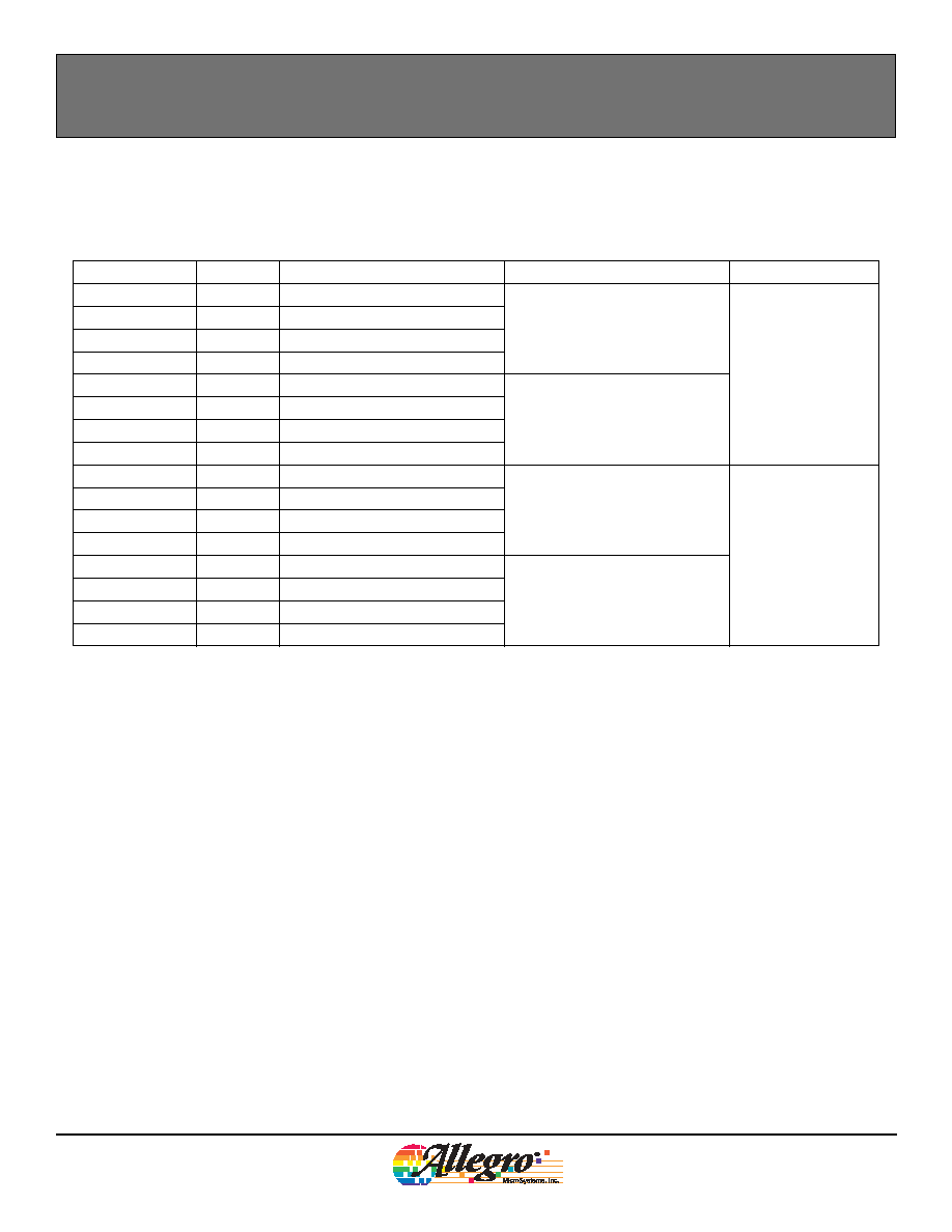
Electrical Operating Characteristics, Package L
I
CC(off)
0
1
2
3
4
5
6
7
8
-50
0
50
100
150
200
Temperature (
∞
C)
Cu
rr
en
t (mA)
3.3 V
18 V
0
1
2
3
4
5
6
7
8
0
5
10
15
20
V
CC
(V)
Cu
rre
n
t
(mA)
-40
∞
C
25
∞
C
150
∞
C
I
CC(on)
0
1
2
3
4
5
6
7
8
-50
0
50
100
150
200
Temperature (
∞
C)
C
u
r
r
en
t
(m
A)
3.3 V
18 V
0
1
2
3
4
5
6
7
8
0
5
10
15
20
V
CC
(V)
C
u
r
r
e
n
t
(mA)
-40
∞
C
25
∞
C
150
∞
C
V
CC
= 3.3 V, I
sink
= 20 mA
0
100
200
300
400
500
-50
0
50
100
150
200
Ch. A
Ch. B
V
sat
(m
V)
Output Saturation Voltage
I
CC(off)
I
CC(on)
Temperature (
∞
C)

12
A3425DS-Rev. !
Worcester, Massachusetts 01615-0036 (508) 853-5000
115 Northeast Cutoff, Box 15036
www.allegromicro.com
Allegro MicroSystems, Inc.
Ultra-Sensitive Dual-Channel Quadrature Hall-Effect Bipolar Switch
A3425
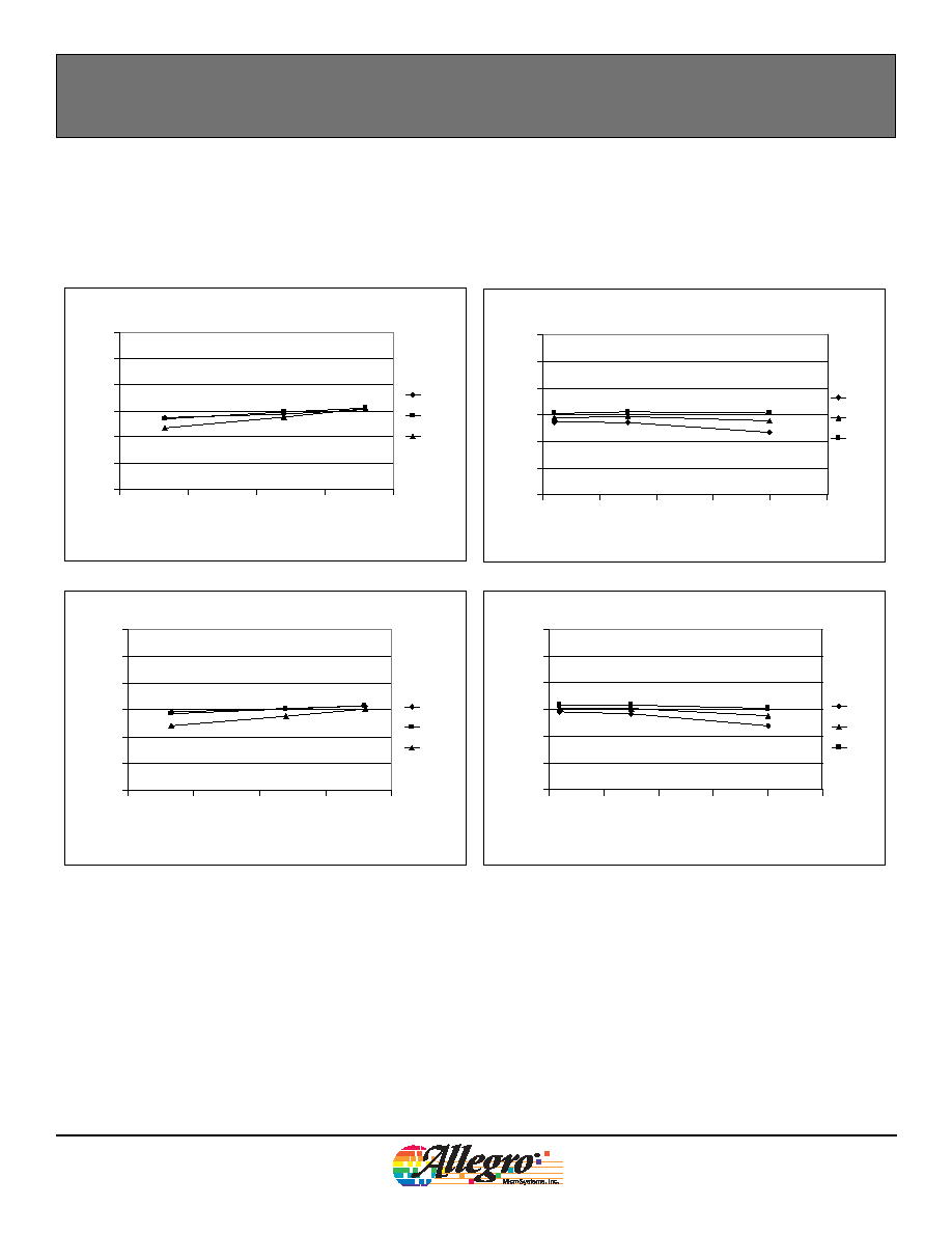
Magnetic Operating Characteristics, Package L
Additional magnetic characteristics on next page
Channel A, B
OP
and B
RP
-30
-20
-10
0
10
20
30
0
5
10
15
20
S
w
i
t
c
h
p
o
i
n
t
(G)
-40
∞
C
25
∞
C
150
∞
C
-30
-20
-10
0
10
20
30
-50
0
50
100
150
200
S
w
i
t
chp
oi
nt
(G)
3.3 V
12 V
18 V
Channel B, B
OP
and B
RP
-30
-20
-10
0
10
20
30
0
5
10
15
20
S
wit
c
h
poi
nt
(G)
-40
∞
C
25
∞
C
150
∞
C
Channel B, B
OP
and B
RP
-30
-20
-10
0
10
20
30
-50
0
50
100
150
200
S
wit
c
h
poi
nt
(G)
3.3 V
12 V
18 V
Channels A and B, Hysteresis
0
5
10
15
20
25
30
0
5
10
15
20
B
OP
- B
RP
(G)
-40
∞
C
25
∞
C
150
∞
C
Channels A and B, Hysteresis
0
5
10
15
20
25
30
-50
0
50
100
150
200
B
OP
- B
RP
(G)
3.3 V
12 V
18 V
Channel A, B
OP
and B
RP
B
OP
B
RP
B
OP
B
RP
B
OP
B
RP
B
OP
B
RP
V
CC
(V)
Temperature (
∞
C)
V
CC
(V)
Temperature (
∞
C)
V
CC
(V)
Temperature (
∞
C)
13
A3425DS-Rev. !
Worcester, Massachusetts 01615-0036 (508) 853-5000
115 Northeast Cutoff, Box 15036
www.allegromicro.com
Allegro MicroSystems, Inc.
Ultra-Sensitive Dual-Channel Quadrature Hall-Effect Bipolar Switch
A3425
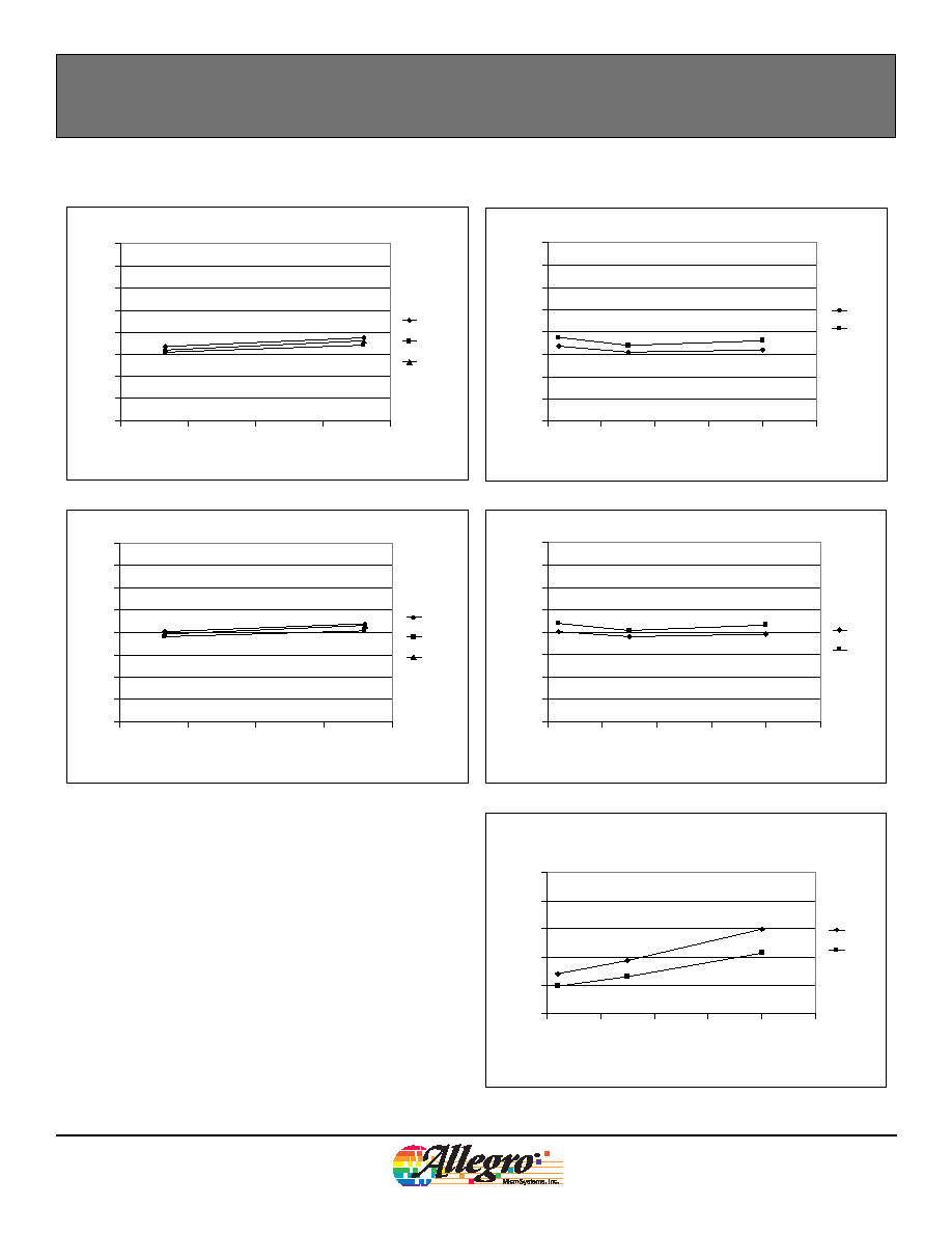
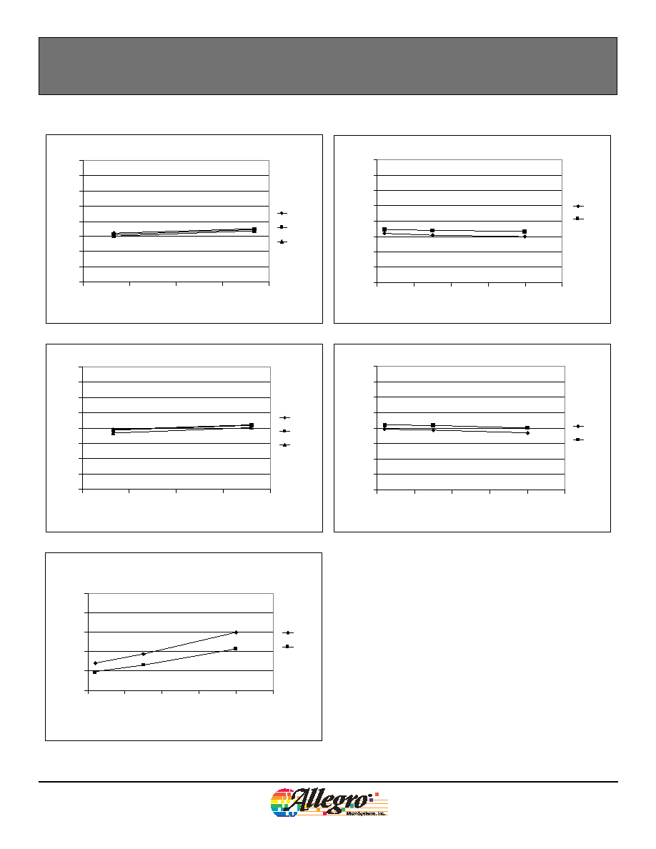
Magnetic Operating Characteristics, Package L (continued)
Additional magnetic characteristics on next page
B
OP
Symmetry
-30
-20
-10
0
10
20
30
0
5
10
15
20
V
CC
(V)
Ch. A -
Ch. B (G)
-40
∞
C
25
∞
C
150
∞
C
B
OP
Symmetry
-30
-20
-10
0
10
20
30
-50
0
50
100
150
200
Temperature (
∞
C)
Ch. A -
Ch. B (G)
3.3 V
12 V
18 V
B
RP
Symmetry
-30
-20
-10
0
10
20
30
0
5
10
15
20
V
CC
(V)
Ch. A -
Ch. B (G)
-40
∞
C
25
∞
C
150
∞
C
B
RP
Symmetry
-30
-20
-10
0
10
20
30
-50
0
50
100
150
200
Temperature (
∞
C)
Ch. A -
Ch. B (G)
3.3 V
12 V
18 V
14
A3425DS-Rev. !
Worcester, Massachusetts 01615-0036 (508) 853-5000
115 Northeast Cutoff, Box 15036
www.allegromicro.com
Allegro MicroSystems, Inc.
Ultra-Sensitive Dual-Channel Quadrature Hall-Effect Bipolar Switch
A3425
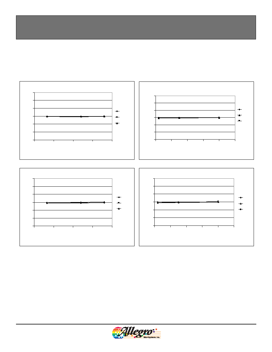
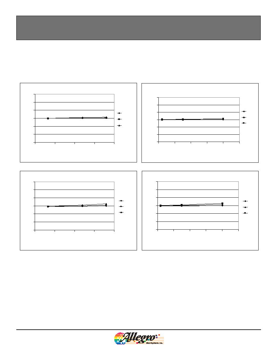
Magnetic Operating Characteristics, Package L (continued)
Ch. A Symmetry
-30
-20
-10
0
10
20
30
0
5
10
15
20
V
CC
(V)
B
OP
+ B
RP
(G)
-40
∞
C
25
∞
C
150
∞
C
Ch. A Symmetry
-30
-20
-10
0
10
20
30
-50
0
50
100
150
200
Temperature (
∞
C)
B
OP
+ B
RP
(G)
3.3 V
12 V
18 V
Ch. B Symmetry
-30
-20
-10
0
10
20
30
0
5
10
15
20
V
CC
(V)
B
OP
+ B
RP
(G)
-40
∞
C
25
∞
C
150
∞
C
Ch. B Symmetry
3.3 V
12 V
18 V
-30
-20
-10
0
10
20
30
-50
0
50
100
150
200
Temperature (
∞
C)
B
OP
+ B
RP
(G)
15
A3425DS-Rev. !
Worcester, Massachusetts 01615-0036 (508) 853-5000
115 Northeast Cutoff, Box 15036
www.allegromicro.com
Allegro MicroSystems, Inc.
Ultra-Sensitive Dual-Channel Quadrature Hall-Effect Bipolar Switch
A3425
Electrical Operating Characteristics, Package K
I
CC(off)
0
1
2
3
4
5
6
7
8
-50
0
50
100
150
200
Temperature (
∞
C)
Cu
rr
en
t (mA)
3.3 V
18 V
0
1
2
3
4
5
6
7
8
0
5
10
15
20
V
CC
(V)
Cu
rre
n
t
(mA)
-40
∞
C
25
∞
C
150
∞
C
I
CC(on)
0
1
2
3
4
5
6
7
8
-50
0
50
100
150
200
Temperature (
∞
C)
C
u
r
r
en
t
(m
A)
3.3 V
18 V
0
1
2
3
4
5
6
7
8
0
5
10
15
20
V
CC
(V)
C
u
r
r
e
n
t
(mA)
-40
∞
C
25
∞
C
150
∞
C
I
CC(off)
I
CC(on)
V
CC
= 3.3 V, I
sink
= 20 mA
0
100
200
300
400
500
-50
0
50
100
150
200
Ch. A
Ch. B
V
sat
(m
V)
Output Saturation Voltage
Temperature (
∞
C)

16
A3425DS-Rev. !
Worcester, Massachusetts 01615-0036 (508) 853-5000
115 Northeast Cutoff, Box 15036
www.allegromicro.com
Allegro MicroSystems, Inc.
Ultra-Sensitive Dual-Channel Quadrature Hall-Effect Bipolar Switch
A3425
Magnetic Operating Characteristics, Package K
Additional magnetic characteristics on next page
Channel A, B
OP
and B
RP
-30
-20
-10
0
10
20
30
0
5
10
15
20
S
w
i
t
c
h
p
o
i
n
t
(G)
-40
∞
C
25
∞
C
150
∞
C
-30
-20
-10
0
10
20
30
-50
0
50
100
150
200
S
w
i
t
chp
oi
nt
(G)
3.3 V
12 V
18 V
Channel B, B
OP
and B
RP
-30
-20
-10
0
10
20
30
0
5
10
15
20
S
wit
c
h
poi
nt
(G)
-40
∞
C
25
∞
C
150
∞
C
Channel B, B
OP
and B
RP
-30
-20
-10
0
10
20
30
-50
0
50
100
150
200
S
wit
c
h
poi
nt
(G)
3.3 V
12 V
18 V
Channels A and B, Hysteresis
0
5
10
15
20
25
30
0
5
10
15
20
B
OP
- B
RP
(G)
-40
∞
C
25
∞
C
150
∞
C
Channels A and B, Hysteresis
0
5
10
15
20
25
30
-50
0
50
100
150
200
B
OP
- B
RP
(G)
3.3 V
12 V
18 V
Channel A, B
OP
and B
RP
B
OP
B
RP
B
OP
B
RP
B
OP
B
RP
B
OP
B
RP
V
CC
(V)
Temperature (
∞
C)
V
CC
(V)
Temperature (
∞
C)
V
CC
(V)
Temperature (
∞
C)
17
A3425DS-Rev. !
Worcester, Massachusetts 01615-0036 (508) 853-5000
115 Northeast Cutoff, Box 15036
www.allegromicro.com
Allegro MicroSystems, Inc.
Ultra-Sensitive Dual-Channel Quadrature Hall-Effect Bipolar Switch
A3425
Magnetic Operating Characteristics, Package K (continued)
Additional magnetic characteristics on next page
B
OP
Symmetry
-30
-20
-10
0
10
20
30
0
5
10
15
20
V
CC
(V)
Ch. A -
Ch. B (G)
-40
∞
C
25
∞
C
150
∞
C
B
OP
Symmetry
-30
-20
-10
0
10
20
30
-50
0
50
100
150
200
Temperature (
∞
C)
Ch. A -
Ch. B (G)
3.3 V
12 V
18 V
B
RP
Symmetry
-30
-20
-10
0
10
20
30
0
5
10
15
20
V
CC
(V)
Ch. A -
Ch. B (G)
-40
∞
C
25
∞
C
150
∞
C
B
RP
Symmetry
-30
-20
-10
0
10
20
30
-50
0
50
100
150
200
Temperature (
∞
C)
Ch. A -
Ch. B (G)
3.3 V
12 V
18 V

18
A3425DS-Rev. !
Worcester, Massachusetts 01615-0036 (508) 853-5000
115 Northeast Cutoff, Box 15036
www.allegromicro.com
Allegro MicroSystems, Inc.
Ultra-Sensitive Dual-Channel Quadrature Hall-Effect Bipolar Switch
A3425
Magnetic Operating Characteristics, Package K (continued)
Ch. A Symmetry
-30
-20
-10
0
10
20
30
0
5
10
15
20
V
CC
(V)
B
OP
+ B
RP
(G)
-40
∞
C
25
∞
C
150
∞
C
Ch. A Symmetry
-30
-20
-10
0
10
20
30
-50
0
50
100
150
200
Temperature (
∞
C)
B
OP
+ B
RP
(G)
3.3 V
12 V
18 V
Ch. B Symmetry
-30
-20
-10
0
10
20
30
0
5
10
15
20
V
CC
(V)
B
OP
+ B
RP
(G)
-40
∞
C
25
∞
C
150
∞
C
Ch. B Symmetry
3.3 V
12 V
18 V
-30
-20
-10
0
10
20
30
-50
0
50
100
150
200
Temperature (
∞
C)
B
OP
+ B
RP
(G)
19
A3425DS-Rev. !
Worcester, Massachusetts 01615-0036 (508) 853-5000
115 Northeast Cutoff, Box 15036
www.allegromicro.com
Allegro MicroSystems, Inc.
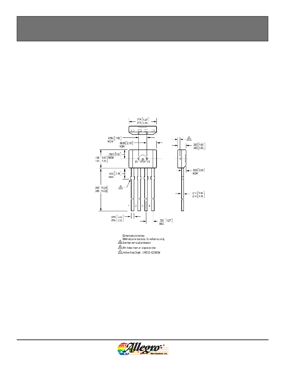
Ultra-Sensitive Dual-Channel Quadrature Hall-Effect Bipolar Switch
A3425
Package K, 4-pin SIP

20
A3425DS-Rev. !
Worcester, Massachusetts 01615-0036 (508) 853-5000
115 Northeast Cutoff, Box 15036
www.allegromicro.com
Allegro MicroSystems, Inc.
Ultra-Sensitive Dual-Channel Quadrature Hall-Effect Bipolar Switch
A3425
Package L, 8-pin SOIC

21
A3425DS-Rev. !
Worcester, Massachusetts 01615-0036 (508) 853-5000
115 Northeast Cutoff, Box 15036
www.allegromicro.com
Allegro MicroSystems, Inc.
Ultra-Sensitive Dual-Channel Quadrature Hall-Effect Bipolar Switch
A3425
The products described herein are manufactured under one
or more of the following U.S. patents: 5,045,920; 5,264,783;
5,442,283; 5,389,889; 5,581,179; 5,517,112; 5,619,137; 5,621,319;
5,650,719; 5,686,894; 5,694,038; 5,729,130; 5,917,320; and other
patents pending.
Allegro MicroSystems, Inc. reserves the right to make, from time
to time, such de par tures from the detail spec i fi ca tions as may be
required to permit improvements in the per for mance, reliability,
or manufacturability of its products. Before placing an order, the
user is cautioned to verify that the information being relied upon is
current.
Allegro products are not authorized for use as critical compo-
nents in life-support devices or sys tems without express written
approval.
The in for ma tion in clud ed herein is believed to be ac cu rate and
reliable. How ev er, Allegro MicroSystems, Inc. assumes no re spon -
si bil i ty for its use; nor for any in fringe ment of patents or other
rights of third parties which may result from its use.
Copyright © 2005, Allegro MicroSystems, Inc.