 | –≠–ª–µ–∫—Ç—Ä–æ–Ω–Ω—ã–π –∫–æ–º–ø–æ–Ω–µ–Ω—Ç: A3516LUA | –°–∫–∞—á–∞—Ç—å:  PDF PDF  ZIP ZIP |

NOTE: For detailed information on purchasing options, contact your
local Allegro field applications engineer or sales representative.
Allegro MicroSystems, Inc. reserves the right to make, from time to time, revisions to the anticipated product life cycle plan for a
product to accommodate changes in production capabilities, alternative product availabilities, or market demand. The information
included herein is believed to be accurate and reliable. However, Allegro MicroSystems, Inc. assumes no responsibility for its use; nor
for any infringements of patents or other rights of third parties which may result from its use.
Recommended Substitutions:
Ratiometric, Linear Hall-Effect Sensors
for High-Temperature Operation
A3515 and A3516
For new customers or new applications:
∑ for the A3515, please refer to the Allegro
A
1321
, and
∑ for the A3516, please refer to the Allegro
A
1323
.
Date of status change: May 2, 2005
These parts are in production but have been determined to be
NOT FOR NEW DESIGN. This classification indicates that sale of
this device is currently restricted to existing customer applications.
The device should not be purchased for new design applications
because obsolescence in the near future is probable. Samples are no
longer available.
Not for New Design

The A3515≠ and A3516≠ are sensitive, temperature-stable linear Hall-
effect sensors with greatly improved offset characteristics. Ratiometric, linear
Hall-effect sensors provide a voltage output that is proportional to the applied
magnetic field and have a quiescent output voltage that is approximately 50%
of the supply voltage. These magnetic sensors are ideal for use in linear and
rotary position sensing systems in the harsh environments of automotive and
industrial applications over extended temperatures to -40
∞
C and +150
∞
C. The
A3515≠ features an output sensitivity of 5 mV/G, while the A3516≠ has an
output sensitivity of 2.5 mV/G. See the Magnetic Characteristics table for
complete, individual device parametrics.
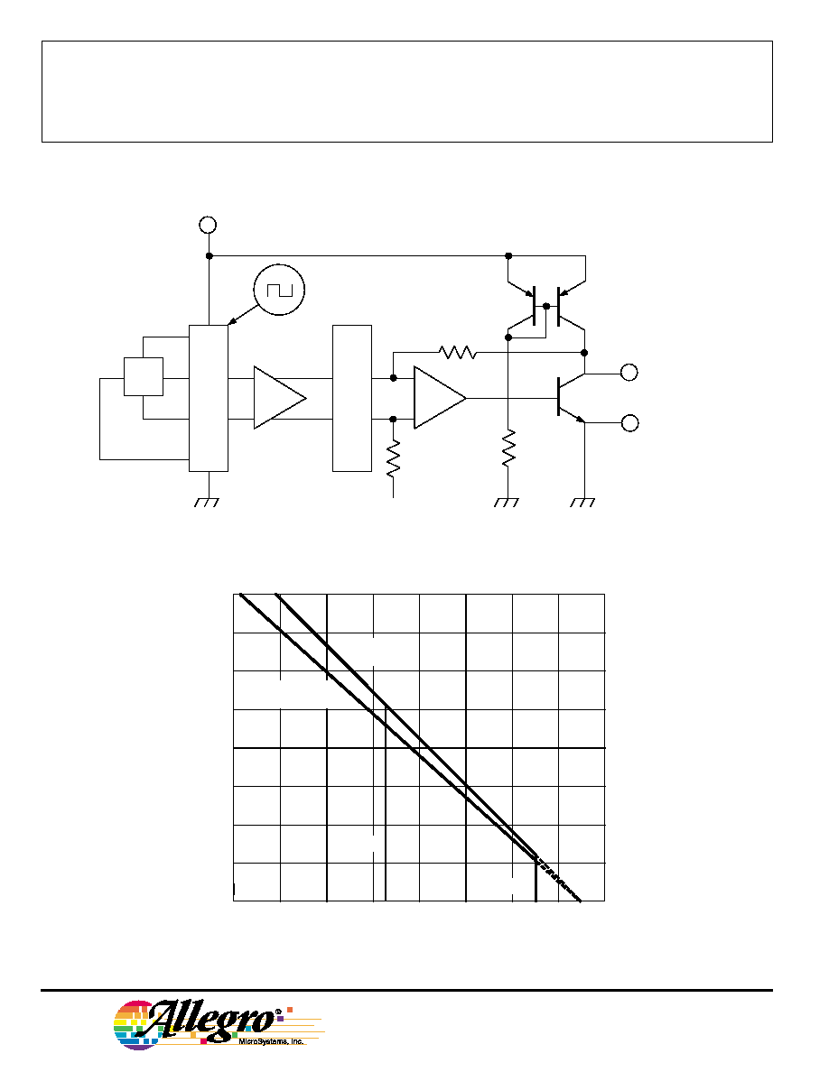
Each BiCMOS monolithic circuit integrates a Hall element, improved
temperature-compensating circuitry to reduce the intrinsic sensitivity drift of
the Hall element, a small-signal high-gain amplifier, and a rail-to-rail low-
impedance output stage.
A proprietary dynamic offset cancelation technique, with an internal
high-frequency clock, reduces the residual offset voltage, which is normally
caused by device overmolding, temperature dependancies, and thermal stress.
This technique produces devices that have an extremely stable quiescent
output voltage, are immune to mechanical stress, and have precise recover-
ability after temperature cycling. Many problems normally associated with
low-level analog signals are minimized by having the Hall element and
amplifier in a single chip. Output precision is obtained by internal gain and
offset trim adjustments during the manufacturing process.
These devices are supplied in a 3-pin ultra-mini-SIP `UA' package.
FEATURES
s Temperature-Stable Quiescent Output Voltage
s Precise Recoverability After Temperature Cycling
s Output Voltage Proportional to Applied Magnetic Field
s Ratiometric Rail-to-Rail Output
s Improved Sensitivity
s 4.5 V to 5.5 V Operation
s Immune to Mechanical Stress
s Small Package Size
s Solid-State Reliability
RATIOMETRIC, LINEAR HALL-EFFECT SENSORS
FOR HIGH-TEMPERATURE OPERATION
Data Sheet
27501.10C
3515
AND
3516
Always order by complete part number, e.g., A3515LUA .
Pinning is shown viewed from branded side.
ABSOLUTE MAXIMUM RATINGS
Supply Voltage, V
CC
.............................. 8.0 V
Output Voltage, V
O
................................ 8.0 V
Output Sink Current, I
O
....................... 10 mA
Magnetic Flux Density, B .............. Unlimited
Package Power Dissipation,
P
D
........................................... See Graph
Operating Temperature Range*, T
A
Suffix `E≠' ..................... -40
∞
C to +85
∞
C
Suffix `L≠' .................... -40
∞
C to +150
∞
C
Storage Temperature Range,
T
S
.................................. -65
∞
C to +170
∞
C
* Infrequent excursions permitted; see
Applications Information.
Dwg. PH-006
1
SUPPLY
V
CC
GROUND
3
2
OUTPUT
X
3515
AND
3516
RATIOMETRIC,
LINEAR
HALL-EFFECT SENSORS
115 Northeast Cutoff, Box 15036
Worcester, Massachusetts 01615-0036 (508) 853-5000
2
Dwg. FH-016A
GROUND
2
OUTPUT
3
1
X
DYNAMIC
OFFSET CANCELLATION
LOW-PASS
FILTER
≠
+
≠
+
SUPPLY
Vcc
Vcc/2
600
400
200
20
60
100
140
0
AMBIENT TEMPERATURE in
∞
∞
∞
∞
C
ALLOWABLE PACKAGE POWER DISSIPATION in MILLIWATTS
Dwg. GH-046A
Suffix "≠UA"
R
JA
= 165
∞
C/W
40
80
120
180
700
500
300
100
160
800
Suffix "E≠"
Suffix "L≠"
Suffix "≠U"
R
JA
= 184
∞
C/W
Copyright © 1996, 2003 Allegro MicroSystems, Inc.
FUNCTIONAL BLOCK DIAGRAM
∞

3515
AND
3516
RATIOMETRIC,
LINEAR
HALL-EFFECT SENSORS
www.allegromicro.com
3
ELECTRICAL CHARACTERISTICS over operating temperature range, at V
CC
= 5 V (unless
otherwise noted).
Limits
Characteristic
Symbol
Test Conditions
Min.
Typ.
Max.
Units
Supply Voltage
V
CC
Operating
4.5
5.0
5.5
V
Supply Current
I
CC
B = 0, V
CC
= 6 V, I
O
= 0
≠
7.2
10
mA
Quiescent
V
OQ
B = 0, I
O
= 1 mA, T
A
= 25
∞
C
2.425
2.500
2.575
V
Voltage Output
Output Voltage
V
OH
B = +X*, I
O
= 1 mA
≠
4.7≠
V
V
OL
B = -X*, I
O
= -1 mA
≠
0.2
≠
V
Output
I
OLM
B = -X*, V
O
= 0
-1.0
-1.5
≠
mA
Source Current Limit
Bandwidth (-3 dB)
BW
≠
30
≠
kHz
Clock Frequency
f
C
≠
170
≠
kHz
Output Resistance
r
O
I
O
-2 mA
≠
1.0
≠
Wide-Band
e
o
B = 0, BW = 10 Hz to 10 kHz,
≠
400
≠
µ
V
Output Noise (rms)
I
O
-1 mA, C
O
= 100 pF
NOTE 1 ≠ Typical data is at T
A
= 25
∞
C and is for design information only.
NOTE 2 ≠ Negative current is defined as coming out of (sourcing) the output.
* This test requires positive and negative fields sufficient to swing the output driver between fully OFF and saturated (ON), respec-
tively. It is NOT intended to indicate a range of linear operation.
3515
AND
3516
RATIOMETRIC,
LINEAR
HALL-EFFECT SENSORS
115 Northeast Cutoff, Box 15036
Worcester, Massachusetts 01615-0036 (508) 853-5000
4
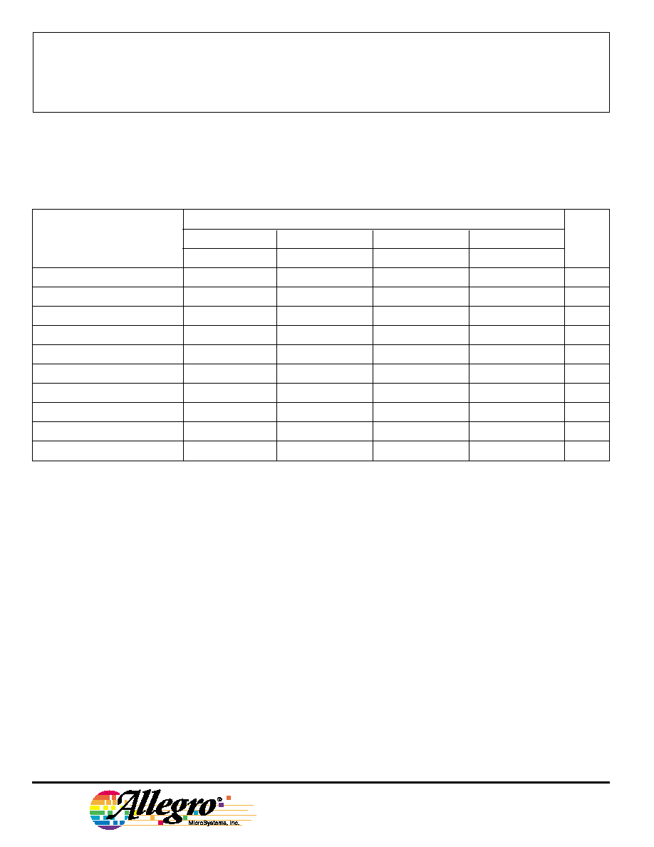
MAGNETIC CHARACTERISTICS over operating temperature range, at V
CC
= 5 V, I
O
= -1 mA
(unless otherwise noted).
Part Numbers
A3515EUA
A3515LUA
A3516EUA
A3516LUA
Characteristic*
Min. Typ. Max.
Min. Typ. Max.
Min. Typ. Max.
Min. Typ. Max.
Units
Operating Temp. Range, T
A
-40
≠
+85
-40
≠
+150
-40
≠
+85
-40
≠
+150
∞
C
Sensitivity
at T
A
= 25
∞
C
4.50 5.00 5.50
4.50 5.00 5.50
2.25 2.50 2.75
2.25 2.50 2.75
mV/G
Sens
(
T)
at T
A
= Max.
-2.5
2.5
7.5
-2.5
2.5
7.5
-2.5
2.5
7.5
-2.5
2.5
7.5
%
Sens
(
T)
at T
A
= Min.
-9.0
-1.3
1.0
-9.0
-1.3
1.0
-9.0
-1.3
1.0
-9.0
-1.3
1.0
%
V
OQ(
T)
≠
≠
±
10
≠
≠
±
10
≠
≠
±
10
≠
≠
±
10
G
Ratiometry,
V
OQ(
V)
≠
100
≠
≠
100
≠
≠
100
≠
≠
100
≠
%
Ratiometry,
Sens
(
V)
≠
100
≠
≠
100
≠
≠
100
≠
≠
100
≠
%
Positive Linearity, Lin+
≠
100
≠
≠
100
≠
≠
100
≠
≠
100
≠
%
Negative Linearity, Lin≠
≠
100
≠
≠
100
≠
≠
100
≠
≠
100
≠
%
Symmetry
≠
100
≠
≠
100
≠
≠
100
≠
≠
100
≠
%
NOTE 1 ≠ Magnetic flux density is measured at most sensitive area of device located 0.0195" (0.50 mm) below the branded face of
the "UA" package.
NOTE 2 ≠ 10 G = 1 mT, exactly.
NOTE 3 ≠ Except for
Sens
(
T)
, typical data is at T
A
= 25
∞
C and is for design information only.
* See Characteristics Definitions for test conditions.
This calculation (formula 1, next page) yields the device's equivalent accuracy, over the operating temperature range, in gauss.