 | –≠–ª–µ–∫—Ç—Ä–æ–Ω–Ω—ã–π –∫–æ–º–ø–æ–Ω–µ–Ω—Ç: A3935KJP | –°–∫–∞—á–∞—Ç—å:  PDF PDF  ZIP ZIP |

Always order by complete part number, e.g., A3935KLQ .
Data Sheet
26301.102
b
3-PHASE POWER MOSFET CONTROLLER
-- For Automotive Applications
3935
The A3935 is designed specifically for automotive applications that
require high-power motors. Each provides six high-current gate drive
outputs capable of driving a wide range of n-channel power MOSFETs.
A requirement of automotive systems is steady operation over a
varying battery input range. The A3935 integrates a pulse-frequency
modulated boost converter to create a constant supply voltage for
driving the external MOSFETs. Bootstrap capacitors are utilized to
provide the above battery supply voltage required for n-channel FETs.
Direct control of each gate output is possible via six TTL-compat-
ible inputs. A differential amplifier is integrated to allow accurate
measurement of the current in the three-phase bridge.
Diagnostic outputs can be continuously monitored to protect the
driver from short-to-battery, short-to-supply, bridge-open, and battery
under/overvoltage conditions. Additional protection features include
dead-time, VDD undervoltage, and thermal shutdown.
The A3935 is supplied in a choice of three packages, a 44-lead
PLCC with copper batwing tabs (suffix ED), a 48-lead low profile QFP
with exposed thermal pad (suffix JP), and a 36-lead 0.8 mm pitch SOIC
(suffix LQ).
FEATURES
!
!
!
!
!
Drives wide range of n-channel MOSFETs in 3-phase bridges
!
!
!
!
!
PFM boost converter for use with low-voltage battery supplies
!
!
!
!
!
Internal LDO regulator for gate-driver supply
!
!
!
!
!
Bootstrap circuits for high-side gate drivers
!
!
!
!
!
Current monitor output
!
!
!
!
!
Adjustable battery overvoltage detection.
!
!
!
!
!
Diagnostic outputs
!
Motor lead short-to-battery, short-to-ground, and
bridge-open protection
!
Undervoltage protection
!
!
!
!
!
-40 ∞C to +150 ∞C, T
J
operation
!
!
!
!
!
Thermal shutdown
ABSOLUTE MAXIMUM RATINGS
Load Supply Voltages, VBAT, VDRAIN,
VBOOST, BOOSTD ... -0.6 V to 40 V
Output Voltage Ranges,
GHA/GHB/GHC, V
GHX
.. -4 V to 55 V
SA/SB/SC, V
SX
............... -4 V to 40 V
GLA/GLB/GLC, V
GLX
.... -4 V to 16 V
CA/CB/CC, V
CX
.......... -0.6 V to 55 V
Sense Circuit Voltages,
CSP,CSN, LSS ............... -4 V to 6.5 V
Logic Supply Voltage,
V
DD
........................... -0.3 V to +6.5 V
Logic Input/Outputs and OVSET, BOOSTS,
CSOUT, VDSTH ......... -0.3 V to 6.5 V
Operating Temperature Range,
T
A
........................... -40∞C to +135∞C
Junction Temperature, T
J
........... +150∞C
Storage Temperature Range,
T
S
........................... -55∞C to +150∞C
* Fault conditions that produce excessive
junction temperature will activate device
thermal shutdown circuitry. These conditions
can be tolerated, but should be avoided.
Package ED, 44-Pin PLCC
Package JP, 48-Pin LQFP
Package LQ, 36-Pin SOIC

3935
THREE-PHASE POWER
MOSFET CONTROLLER
115 Northeast Cutoff, Box 15036
Worcester, Massachusetts 01615-0036 (508) 853-5000
2
Functional Block Diagram
Copyright © 2003 Allegro MicroSystems, Inc.
See pages 8 and 9 for terminal assignments and descriptions.
3935
THREE-PHASE POWER
MOSFET CONTROLLER
www.allegromicro.com
3
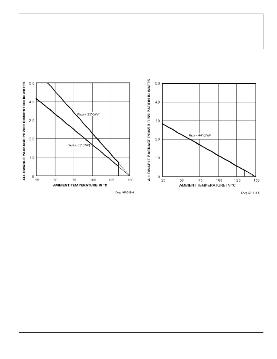
* Measured on "High-K" multi-layer PWB per JEDEC Standard JESD51-7.
Measured on typical two-sided PWB with power tabs (terminals 1, 2, 11, 12, 22, 23, 34, and 35) connected to copper foil with an
area of 3.8 square inches (2452 mm
2
) on each side. See Application Note 29501.5, Improving Batwing Power Dissipation, for
additional information.
A3935KLQ (SOIC)
A3935KED (PLCC)
3935
THREE-PHASE POWER
MOSFET CONTROLLER
115 Northeast Cutoff, Box 15036
Worcester, Massachusetts 01615-0036 (508) 853-5000
4
ELECTRICAL CHARACTERISTICS:
unless otherwise noted at T
J
= -40∞C to +150∞C, V
BAT
= 7 V to 16 V,
V
DD
= 4.75 V to 5.25 V, ENABLE = 22.5 kHz, 50% Duty Cycle, Two Phases Active.
Limits
Characteristics
Symbol
Conditions
Min
Typ
Max
Units
Power Supply
V
DD
Supply Current
I
DD
All logic inputs = 0 V
≠
≠
7.0
mA
V
BAT
Supply Current
I
BAT
All logic inputs = 0 V
≠
≠
3.0
mA
Battery Voltage Operating Range
V
BAT
7.0
≠
40
V
Bootstrap Diode Forward Voltage
V
DBOOT
I
DBOOT
= -I
cx
= 10 mA, V
DBOOT
= V
REG
≠ V
CX
0.8
≠
2.0
V
I
DBOOT
= -I
cx
= 100 mA
1.5
≠
2.3
V
Bootstrap Diode Resistance
r
DBOOT
r
D
(100 mA) = [V
D
(150 mA) ≠ V
D
(50 mA)]/100 mA
2.5
≠
7.5
Bootstrap Diode Current Limit
I
DM
3 V < [V
REG
≠ V
CX
] < 12 V
-150
≠
-1150
mA
Bootstrap Quiescent Current
I
CX
V
CX
= 40 V, GHx = ON
10
≠
30
µA
Bootstrap Refresh Time
t
refresh
V
SX
= low to guarantee
V = +0.5 V refresh of
≠
≠
2.0
µs
0.47 µF Boot Cap at V
cx
≠ V
sx
= +10 V
VREG Output Voltage
1
V
REG
V
BAT
= 7 V to 40 V, V
BOOST
from Boost Reg
12.7
≠
14
V
VREG Dropout Voltage
2
V
REGDO
V
REGDO
= V
boost
≠ V
reg
, I
reg
= 40 mA
≠
0.9
≠
V
Gate Drive Avg. Supply Current
I
REG
No external dc load at VREG, C
REG
= 10 µF
≠
≠
40
mA
VREG Input Bias Current
I
REGBIAS
Current into V
BOOST
, ENABLE = 0
≠
≠
4.0
mA
Boost Supply
V
BOOST
Output Voltage Limit
V
BOOSTM
V
BAT
= 7 V
14.9
≠
16.3
V
V
BOOST
Output Volt. Limit Hyst.
V
BOOSTM
35
≠
180
mV
Boost Switch ON Resistance
r
DS(on)
I
BOOSTD
< 300 mA
≠
1.4
3.3
Max. Boost Switch Current
I
BOOSTSW
≠
≠
300
mA
Boost Current Limit Threshold Volt.
V
BI(th)
Increasing V
BOOSTS
0.45
≠
0.55
V
OFF Time
t
off
3.0
≠
8.0
µs
Blanking Time
t
blank
100
≠
220
ns
NOTES: Typical Data and Typical Characteristics are for design information only.
Negative current is defined as coming out of (sourcing) the specified device terminal.
1. For V
BOOSTM
< V
BOOST
< 40 V power dissipation in the V
REG
LDO increases. Observe T
J
< 150 ∞C limit.
2. With V
BOOST
decreasing Dropout Voltage measured at V
REG
= V
REGref
≠ 200 mV where V
REG(ref)
= V
REG
at V
BOOST
= 16 V.
Continued next page ...
3935
THREE-PHASE POWER
MOSFET CONTROLLER
www.allegromicro.com
5
Characteristics
Symbol
Conditions
Limits
Min
Typ
Max
Units
Control Logic
Logic Input Voltages
V
I(1)
Minimum high level input for logical "one"
2.0
≠
≠
V
V
I(0)
Maximum low level input for logical "zero"
≠
≠
0.8
V
Logic Input Currents
I
I(1)
V
I
= V
DD
≠
≠
500
µA
I
I(0)
V
I
= 0.8 V
50
≠
≠
µA
Input Hysteresis
V
hys
100
≠
300
mV
Logic Output High Voltage
V
O(H)
I
O(H)
= -800 µA
V
DD
≠ 0.8
≠
≠
V
Logic Output Low Voltage
V
I(L)
I
O(L)
= 1.6 mA
≠
≠
0.4
V
Gate Drives, GHx ( internal SOURCE or upper switch stages)
Output High Voltage
V
DSL(H)
GHx: I
xU
= ≠10 mA, V
sx
= 0
V
REG
≠ 2.26
≠
V
REG
V
GLx: I
xU
= ≠10 mA, V
lss
= 0
V
REG
≠ 0.26
≠
V
REG
V
Source Current (pulsed)
I
xU
V
SDU
= 10 V, T
J
= 25 ∞C
≠
800
≠
mA
V
SDU
= 10 V, T
J
= 135 ∞C
400
≠
≠
mA
Source ON Resistance
r
SDU(on)
I
xU
= ≠150 mA, T
J
= 25 ∞C
4.0
≠
10
I
xU
= ≠150 mA, T
J
= 35 ∞C
7.0
≠
15
Gate Drives, GLx ( internal SINK or lower switch stages)
Sink Current (pulsed)
I
xL
V
DSL
= 10 V, T
J
= 25 ∞C
≠
850
≠
mA
V
DSL
= 10 V, T
J
= 135 ∞C
550
≠
≠
mA
Sink ON Resistance
r
DSL(on)
I
xL
= +150 mA, T
J
= 25 ∞C
1.8
≠
6.0
I
xL
= +150 mA, T
J
= 135 ∞C
3.0
≠
7.5
Gate Drives, GHx, GLx (General)
Phase Leakage (Source)
I
Sx
ENABLE = 0, V
Sx
= 1.7 V
0
≠
100
µA
Propagation Delay, Logic only
t
pd
Logic input to unloaded GHx, GLx
≠
≠
150
ns
Output Skew Time
t
sk(o)
Grouped by edge, phase-to-phase
≠
≠
50
ns
Dead Time (Shoot-Through
Prevention)
t
dead
Between GHx, GLx transitions of same phase
75
≠
180
ns
NOTES: Typical Data and Typical Characteristics are for design information only.
Negative current is defi ned as coming out of (sourcing) the specifi ed device terminal.
For
GH
X
: V
SDU
= V
CX
≠ V
GHX
, V
DSL
= V
GHX
≠ V
SX
, V
DSL(H)
= V
CX
≠ V
SDU
≠ V
SX
.
For
GL
X
: V
SDU
= V
REG
≠ V
GLX
, V
DSL
= V
GLX
≠ V
LSS
, V
DSL(H)
= V
REG
≠ V
SDU
≠ V
LSS.
ELECTRICAL CHARACTERISTICS:
unless otherwise noted at T
J
= -40∞C to +150∞C, V
BAT
= 7 V to 16 V,
V
DD
= 4.75 V to 5.25 V, ENABLE = 22.5 kHz, 50% Duty Cycle, Two Phases Active.