 | –≠–ª–µ–∫—Ç—Ä–æ–Ω–Ω—ã–π –∫–æ–º–ø–æ–Ω–µ–Ω—Ç: A3938SEQ | –°–∫–∞—á–∞—Ç—å:  PDF PDF  ZIP ZIP |

Data Sheet
26301.104B
A3938
Three-Phase Power MOSFET Controller
The A3938 is a three-phase, brushless dc motor controller. The A3938
high-current gate drive capability allows driving of a wide range of
power MOSFETs and can support motor supply voltages to 50 V. The
A3938 integrates a bootstrapped high-side driver to minimize the exter-
nal component count required to drive N-channel MOSFET drivers.
Internal fi xed off-time, PWM current-control circuitry can be used to
regulate the maximum load current to a desired value. The peak load
current limit is set by the user's selection of an input reference volt-
age and external sensing resistor. A user-selected external RC timing
network sets the fi xed off-time pulse duration. For added fl exibility, the
PWM input can provide speed/torque control where the internal current
control circuit sets a limit on the maximum current.
The A3938 includes a synchronous rectifi cation feature. This shorts out
the current path through the power MOSFET reverse body diodes dur-
ing PWM off-cycle current decay. This can minimize power dissipation
in the MOSFETs, eliminate the need for external power clamp diodes,
and potentially allow a more economical choice for the MOSFET drivers.
The A3938 provides commutation logic for Hall sensors confi gured for
120-degree spacing. The Hall input pins are pulled-up to an internally-
generated 5 V reference. Power MOSFET protection features include:
bootstrap capacitor charging current monitor, regulator undervoltage
monitor, motor lead short-to-ground, and thermal shutdown.
The LD package is available in a lead-free version (100% matte tin
plated leadframe).
Drives wide range of N-channel MOSFETs
Low-side synchronous rectifi cation
Power MOSFET protection
Adjustable dead time for cross-con-
duction protection
Selectable coast or dynamic brake on
power-down or RESET input
Fast/slow current decay modes
Use the following complete part numbers when ordering:
AB SO LUTE MAX I MUM RAT INGS
Part Number
Pins
Package
A3938SEQ
32
PLCC
A3938SLQ
36
QSOP
A3938SLD
38
TSSOP
A3938SLD-T
38
TSSOP, Lead-free
Load Supply Voltage, V
BB
...................................50 V
VREG (Transient) ...............................................15 V
Logic Input Voltage Range, V
IN
...≠0.3 V to V
LCAP
+0.3 V
Sense Voltage, V
SENSE
........................... ≠5 V to 1.5 V
Pins: SA, SB, SC................................... ≠5 V to 50 V
Pins: GHA, GHB, GHC.................. ≠5 V to V
BB
+ 17 V
Pins: CA, CB, CC ...........................SA/SB/SC + 17 V
Operating Temperature Range
Ambient Temperature, T
A
.............≠20∞C to +85∞C
Junction Temperature, T
J
............................+150∞C
Storage Temperature, T
S
..........≠55∞C to +150∞C
Thermal Impedance (Typical), at T
A
= +25∫C;
measured on a JEDEC-standard "High-K" PCB
A3938EQ,
R
JA
........................................37∞C/W
A3938LD,
R
JA
........................................38∞C/W
A3938LQ, R
JA
........................................44∞C/W
FEATURES
Internal PWM current control
Motor lead short-to-ground
protection
Internal 5 V regulator
Fault diagnostic output
Thermal shutdown
Undervoltage protection
A3938LD, 38-pin TSSOP
A3938EQ, 32-pin PLCC
A3938LQ, 36-pin QSOP
2
Worcester, Massachusetts 01615-0036 (508) 853-5000
115 Northeast Cutoff, Box 15036
www.allegromicro.com
Data Sheet
26301.104B
A3938
Three-Phase Power MOSFET Controller
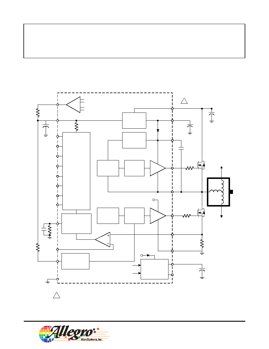
Functional Block Diagram
(This diagram shows only one of the three outputs)
VREG
Regulator
VBB
Charge Pump
Dead-Time
Adjust
RC Blanking
Fixed Off-Time
VREG
Low-Side
Driver
High-Side
Protection
Logic
CA
GHA
SA
DEAD
GLA
PGND
RC
MODE
PWM
SENSE
To Phase B
REF
C
BOOT
DIR
RESET
BRAKE
R
T
C
T
To Phase C
H2
H1
H3
Low-Side
Protection
Logic
R
S
Turn-On
Delay
LCAP
10 uF
0.1 uF
0.1 uF
+
0.1 uF
+
FAULT
AGND
BRKSEL
BRKCAP
Power Loss
Brake
4.7uF
V
REG
UVLO
VREG
RESET
Control
Logic
O.D.
Invalid Hall
VREG Undervoltage
Short to GND
TSD
Turn-On
Delay
High-Side
Driver
+
+
A
A
For 12 V applications, VBB must be shorted to VREG. For this condition, the absolute
maximum rating of 15 V on VREG must be maintained to prevent damage to the A3938.
3
Worcester, Massachusetts 01615-0036 (508) 853-5000
115 Northeast Cutoff, Box 15036
www.allegromicro.com
Data Sheet
26301.104B
A3938
Three-Phase Power MOSFET Controller
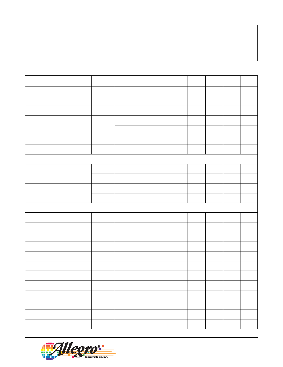
ELECTRICAL CHARACTERISTICS
1,2
Unless otherwise noted: T
A
= 25∞C, V
BB
= 18 V to 50 V, C
LCAP
= 0.1 µF, C
BOOT
= 0.1 µF,
C
VREG
= 10 µF, PWM = 22.5 kHz, square wave, two phases active
Characteristics
Symbol
Test Conditions
Min.
Typ.
1
Max.
Units
Quiescent Current
I
VBB
RESET = 1, Coast mode, stopped
≠
≠
8.0
mA
LCAP Regulator
V
LCAP
I
lcap
= ≠3.0 mA
4.75
5
5.25
V
VREG =VBB Supply Voltage Range
V
REG
VREG = VBB, observe maximum rating = 15 V
10.8
≠
13.2
V
VREG Output Voltage
V
REG
V
BB
= 13.2 V to 18 V, I
vreg
= ≠10 mA
≠
V
BB
≠ 2.5
≠
V
V
BB
= 18 V to 50 V, I
vreg
= ≠10 mA
12.4
13
13.6
V
VREG Load Regulation
V
REGLOAD
I
vreg
= ≠1 mA to ≠30 mA, Coast mode
≠
25
≠
mV
VREG Line Regulation
V
REGLIN
I
vreg
= ≠10 mA, Coast mode
≠
40
≠
mV
Control Logic
Logic Input Voltage
V
IN(1)
Minimum high level for logical 1
2.0
≠
≠
V
V
IN(0)
Maximum low level for logical 0
≠
≠
0.8
V
Logic Input Current
I
IN(1)
V
IN
= 2.0 V
≠30
≠
≠90
µA
I
IN(0)
V
IN
= 0.8 V
≠50
≠
≠130
µA
Gate Drive
Low-Side Drive, Output High
V
HGL
I
gx
= 0
V
REG
≠ 0.8 V
REG
≠ 0.5
≠
V
High-Side Drive, Output High
V
HGH
I
gx
= 0
10.4
11.6
12.8
V
Pull-Up Switch Resistance
R
DS(ON)
I
gx
= ≠50 mA
≠
14
≠
Pull-Down Switch Resistance
R
DS(ON)
I
gx
= 50 mA
≠
4
≠
Low-Side Switching, 10/90 Rise Time
tr
GL
C
load
= 3300 pF
≠
120
≠
ns
Low-Side Switching, 10/90 Fall Time
tf
GL
C
load
= 3300 pF
≠
60
≠
ns
High-Side Switching, 10/90 Rise Time
tr
GH
C
load
= 3300 pF
≠
120
≠
ns
High-Side Switching, 10/90 Fall Time
tf
GH
C
load
= 3300 pF
≠
60
≠
ns
Propagation Delay; GHx,GLx Rising
T
pr
PWM to gate drive out, C
load
= 3300 pF
≠
220
≠
ns
Propagation Delay; GHx,GLx Falling
T
pf
PWM to gate drive out, C
load
= 3300 pF
≠
110
≠
ns
Dead Time, Maximum
t
DEAD
V
dead
= 0, GHx to GLx, C
load
= 0
3.5
5.6
7.6
µs
Dead Time, Minimum
t
DEAD
I
DEAD
= 780 µA, GLx to GHx, C
load
= 0
50
100
150
ns
Continued on next page...
4
Worcester, Massachusetts 01615-0036 (508) 853-5000
115 Northeast Cutoff, Box 15036
www.allegromicro.com
Data Sheet
26301.104B
A3938
Three-Phase Power MOSFET Controller
Characteristics
Symbol
Test Conditions
Min.
Typ.
1
Max.
Units
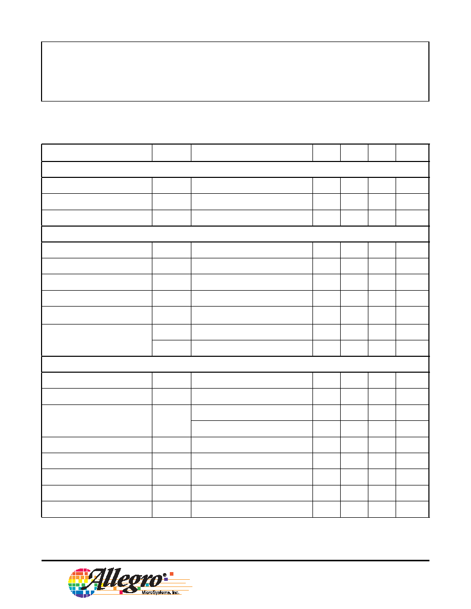
Bootstrap Capacitor
Bootstrap Capacitor Voltage
V
CX
I
cx
= 0, V
sx
= 0, V
reg
= 13 V
10.4
11.6
12.8
V
Bootstrap R
OUT
R
CX
I
cx
= ≠50 mA
≠
9
12
Charge Current (Source)
I
CX
100
≠
≠
mA
Current Limit Circuitry
Input Offset Voltage
V
IO
0 V < V
cmr
< 1.5 V
≠
≠
± 5
mV
Input Current , Sense pin
I
B
0 V < V
cm
, V
diff
< 1.5 V
≠
≠25
≠
µA
Input Current , Reference pin
I
B
0 V < V
cm
, V
diff
< 1.5 V
≠
0
≠
µA
Blank Time
t
BLANK
R = 56 k, C = 470 pF
≠
0.91
≠
µs
RC Charge Current
I
RC
≠0.9
≠1
≠1.1
mA
RC Voltage Threshold
V
RCL
1.0
1.1
1.2
V
V
RCH
2.7
3.0
3.3
V
Protection Circuitry
Bootstrap Charge Threshold
I
cx
GHx turns on, and GLx turns off, at I
cx
≠
≠9
≠
mA
Short to Ground, Drain-Source Monitor
V
dsh
V
BB
≠ V
SX
, high side on
1.3
2.0
2.7
V
VREG Undervoltage Threshold
UVLO
V
REG
increasing
9.2
9.7
10.2
V
V
REG
decreasing
8.6
9.1
9.6
V
Fault Output Voltage
V
OUT
I
OL
= 1 mA
≠
≠
0.5
V
Brake Capacitor Supply Current
I
BRAKE
V
BB
= 8 V, BRKSEL = 1
≠
30
≠
µA
Low Side Gate Voltage
V
GLBH
V
BB
=0, BRKCAP = 8V
≠
6.6
≠
V
Thermal Shutdown Temperature
T
J
≠
165
≠
∞C
Thermal Shutdown Hysteresis
T
J
≠
10
≠
∞C
ELECTRICAL CHARACTERISTICS
1,2
(continued) Unless otherwise noted: T
A
= 25∞C, V
BB
= 18 V to 50 V, C
LCAP
= 0.1 µF,
C
BOOT
= 0.1 µF, C
VREG
= 10 µF, PWM = 22.5 kHz, square wave, two phases active
1
Typical data are for initial design estimations only, and assume optimum manufacturing and application conditions. Performance may vary for
individual units, within the specifi ed maximum and minimum limits.
2
Negative current is defi ned as conventional current coming out of (sourced from) the specifi ed device terminal.

5
Worcester, Massachusetts 01615-0036 (508) 853-5000
115 Northeast Cutoff, Box 15036
www.allegromicro.com
Data Sheet
26301.104B
A3938
Three-Phase Power MOSFET Controller
RESET.
A logic input that enables the device. Has internal
50 k pull-up to LCAP. Setting RESET to 1 coasts or brakes
the motor, depending on the state of the BRKSEL pin. Set-
ting RESET to 0 enables the gate drive to follow commuta-
tion logic. Setting RESET to 1 overrides the BRAKE pin.
GLA/GLB/GLC.
Low-side gate drive outputs for external
MOSFET drivers. External series gate resistors can be used
to control slew rate seen at the power driver gate, thereby
controlling the di/dt and dv/dt of Sx outputs.
SA/SB/SC.
Directly connected to the motor terminals,
these pins sense the voltages switched across the load. The
pins are also connected to the negative side of the bootstrap
capacitors and the negative supply connections for the fl oat-
ing high-side drivers.
GHA/GHB/GHC.
High-side gate drive outputs for
N-channel MOSFET drivers. External series gate resistors
can be used to control slew rate seen at the power driver
gate, thereby controlling the di/dt and dv/dt of Sx outputs.
CA/CB/CC.
High-side connections for bootstrap capaci-
tors, providing positive supply for high-side gate drivers. The
bootstrap capacitors are charged to approximately VREG
when the output Sx terminals go low. When the outputs
swing high, the voltages on these pins rise with the outputs to
provide the boosted gate voltages needed for the N-channel
power MOSFETs.
MODE. Logic input to set current-decay mode. In response
to a PWM Off command, Slow Decay mode (MODE = 1)
switches off the high-side FET, and Fast Decay mode
(MODE = 0) switches off the high-side and low-side FETs.
Has an internal 50 k pull-up to LCAP.
H1/H2/H3.
Hall sensor inputs with internal, 50 k pull-ups
to LCAP. Confi gured for 120-degree electrical spacing.
DIR.
Logic input to reverse rotation (see the table Commu-
tation Truth Table, on the next page). Has internal, 50 k
pull-up to LCAP.
FAULT.
Open-drain output to indicate fault condition. Will
be pulled high (usually by 5.1 k external pull-up) for any of
the following fault conditions:
∑ Invalid Hall sensor input code (coasts the motor).
∑ Undervoltage condition detected at VREG (coasts or brakes
the motor depending on stored setting for BRKSEL).
∑ Thermal shutdown (coasts the motor).
∑ Motor lead (SA/SB/SC) connected to ground (turns off
only the high-side power MOSFETs).
Only the "short-to-ground" fault is latched, but it is cleared
at each commutation. If the motor has stalled due to a short-
to-ground being detected, toggling the RESET pin or repeat-
ing a power-up sequence clears the fault.
BRAKE.
Logic input for braking function. Setting BRAKE
to 1 turns on low-side MOSFETs, and turns off the high-side
MOSFETs. This effectively shorts the BEMF in the windings
and brakes the motor. Internal 50 k pull-up to LCAP. Set-
ting RESET to 1 overrides this BRAKE pin. See also BRKSEL.
BRKCAP.
This pin is for connection of the reservoir
capacitor used to provide the positive power supply for the
sink drive outputs for a power-down condition. This allows
predictable braking, if desired. Using a 4.7
µF capacitor will
provide 6.5 V gate drive for 300 ms. If the power-down brak-
ing option is not needed (i.e., BRKSEL = 0), then this pin
should be tied to VREG.
BRKSEL
. Logic input to enable/disable braking upon
power-down condition or RESET = 1. Internal 50 k pull-up
to LCAP. Setting BRKSEL to 0 enables Coast mode. Setting
BRKSEL to 1 enables Brake mode.
PWM.
Speed control input. Setting PWM to 1 turns on
MOSFETs selected by Hall input logic. Setting PWM to 0
turns off the selected MOSFETs. Keep the PWM input held
high to utilize internal current control circuitry. Internal
50 k pull-up to LCAP.
RC.
Analog input. Connection for R
T
and C
T
to set the
fi xed off-time. C
T
also sets the BLANK time (see the section
Application Information). It is recommended that the fi xed
off-time should not be less than 10 µs. The resistor should be
in the range between 10 k and 500 k.
VREG.
Regulated 13 V supply for the low-side gate drive
and the bootstrap capacitor charge circuit. As a regulator, use
a 10 µF decoupling/storage capacitor (ESR < 1 ) from this
pin to AGND, as close to the device pins as possible.
Note: For 12 V applications, the VREG pin should be
shorted to VBB.
Pin Descriptions