 | –≠–ª–µ–∫—Ç—Ä–æ–Ω–Ω—ã–π –∫–æ–º–ø–æ–Ω–µ–Ω—Ç: A3949 | –°–∫–∞—á–∞—Ç—å:  PDF PDF  ZIP ZIP |
Data Sheet
29319.47C
A3949
DMOS Full-Bridge Motor Driver
Designed for PWM (pulse width modulated) control of dc motors, the
A3949 is capable of peak output currents to ±2.8 A and operating volt-
ages to 36 V.
PHASE and ENABLE input terminals are provided for use in control-
ling the speed and direction of a dc motor with externally applied PWM
control signals. Internal synchronous rectifi cation control circuitry is
provided to reduce power dissipation during PWM operation.
Internal circuit protection includes thermal shutdown with hysteresis,
undervoltage monitoring of V
BB
and V
CP
, and crossover current protec-
tion.
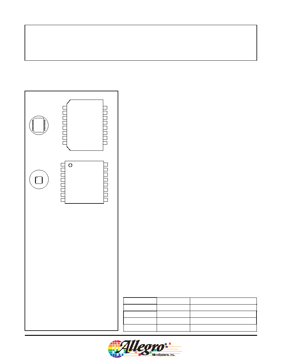
The A3949 is supplied in a choice of two power packages, a 16-pin
plastic SOIC with a copper batwing tab (part number suffi x LB), and
a low profi le (1.1mm) 16-pin TSSOP (suffi x LP) with exposed power
tab. Both packages are available in a lead-free version (100% matte tin
leadframe).
Single supply operation
Very small outline package
Low R
DS(ON)
outputs
Sleep function
Internal UVLO
Crossover current protection
Thermal shutdown protection
Use the following complete part numbers when ordering:
AB SO LUTE MAX I MUM RAT INGS
Part Number
Package
Description
A3949SLB
16-pin, SOIC
Copper batwing tab
A3949SLB-T
16-pin, SOIC
Copper batwing tab; Lead-free
A3949SLP
16-pin, TSSOP
Exposed thermal pad
A3949SLP-T
16-pin, TSSOP
Exposed thermal pad; Lead-free
Load Supply Voltage
V
BB
...............................................................36 V
V
BB
(Peak < 2 µs) ........................................38 V
Output Current, I
OUT
(Repetitive)
1
....................±2.8 A
Sense Voltage, V
SENSE
.........................................0.5 V
Logic Input Voltage, V
IN
..................... ≠0.3 V to 7 V
Package Power Dissipation, P
D
A3949SLB
2
......................................... 52∫C / W
A3949SLP
3
.......................................... 34∫C / W
Operating Temperature Range
Ambient Temperature, T
A
.............≠20∞C to +85∞C
Junction Temperature, T
J
..................+150∞C Max.
Storage Temperature, T
S
..........≠55∞C to +150∞C
1
Output current rating may be limited by duty cycle,
ambient temperature, and heat sinking. Under any set of
conditions,
DO NOT
exceed the specifi ed I
OUT
or T
J
.
2
Measured on a typical two-sided PCB with 2 in.
2
copper
ground plane.
3
Measured on a JEDEC-standard "High-K" 4-layer PCB.
FEATURES
A3949SLB SOIC
A3949SLP TSSOP
3
4
5
6
7
8
2
1
14
13
12
11
10
9
15
16
N/C
MODE
PHASE
GND
SLEEP
ENABLE
OUTA
SENSE
N/C
VREG
VCP
GND
CP2
CP1
OUTB
VBB
3
4
5
6
7
8
2
1
14
13
12
11
10
9
15
16
N/C
MODE
PHASE
GND
SLEEP
ENABLE
OUTA
SENSE
N/C
VREG
VCP
GND
CP2
CP1
OUTB
VBB
Scale 1:1
Scale 1:1
2
Worcester, Massachusetts 01615-0036 (508) 853-5000
115 Northeast Cutoff, Box 15036
www.allegromicro.com
Data Sheet
29319.47C
A3949
DMOS Full-Bridge Motor Driver
Functional Block Diagram
VREG
CP2
Load
Supply
Low Side
Gate Supply
CP1
Charge
Pump
0.1
µF
0.1
µF
DMOS Full Bridge
OSC
.22
µF
25 V
0.1
µF
100
µF
Control
Logic
MODE
PHASE
ENABLE
SLEEP
VCP
VBB
OUTA
OUTB
SENSE
GND
GND
PHASE ENABLE MODE
SLEEP
OUTA
OUTB
Function
1
1
X
1
H
L
Forward
0
1
X
1
L
H
Reverse
X
0
1
1
L
L
Brake (slow decay)
1
0
0
1
L
H
Fast decay SR*
0
0
0
1
H
L
Fast decay SR*
X
X
X
0
Hi-Z
Hi-Z
Sleep mode
Control Logic Table
* To prevent reversal of current during fast decay SR (synchronous rectifi cation), the outputs
go to the high impedance state as the current approaches zero.
3
Worcester, Massachusetts 01615-0036 (508) 853-5000
115 Northeast Cutoff, Box 15036
www.allegromicro.com
Data Sheet
29319.47C
A3949
DMOS Full-Bridge Motor Driver
ELECTRICAL CHARACTERISTICS
at T
A
= 25∞C, V
BB
= 8 V to 36 V (unless otherwise noted)
Characteristics
Symbol
Test Conditions
Min.
Typ.
Max.
Units
Output-On Resistance
R
DSON
Source driver, I
OUT
= ≠2.8 A, T
J
= 25∞C
≠
.4
.48
Source driver, I
OUT
= ≠2.8 A, T
J
= 125∞C
≠
.68
≠
Sink driver, I
OUT
= 2.8 A, T
J
= 25∞C
≠
.3
.43
Sink driver, I
OUT
= ≠2.8 A, T
J
= 125∞C
≠
.576
≠
Body Diode Forward Voltage
V
F
Source diode, I
F
= ≠2.8 A
≠
1.1
1.3
V
Sink diode, I
F
= 2.8 A
≠
1
1.3
V
Motor Supply Current
I
BB
f
PWM
< 50 kHz
≠
6
8.5
mA
Charge pump turned on; outputs disabled
≠
3
4.5
mA
Sleep mode
≠
≠
10
µA
Logic Input Voltage
PHASE, ENABLE, MODE
V
IN(1)
2.0
≠
≠
V
V
IN(0)
≠
≠
0.8
V
Logic Input Voltage
SLEEP
V
IN(1)
2.7
≠
≠
V
V
IN(0)
≠
≠
0.8
V
Logic Input Current
PHASE, MODE pins
I
IN(1)
V
IN
= 2.0 V
≠
< 1.0
20
µA
I
IN(0)
V
IN
= 0.8 V
≠
< ≠2.0
≠20
µA
Logic Input Current
ENABLE pin
I
IN(1)
V
IN
= 2.0 V
≠
40
100
µA
I
IN(0)
V
IN
= 0.8 V
≠
16
40
µA
Logic Input Current
SLEEP pin
I
IN(1)
V
IN
= 2.7 V
≠
27
50
µA
I
IN(0)
V
IN
= 0.8 V
≠
< 1
10
µA
Propagation Delay Times
t
pd
From PWM change to source or sink turn on
≠
600
≠
ns
From PWM change to source or sink turn off
≠
100
≠
ns
Crossover Delay
t
COD
≠
500
≠
ns
Protection Circuitry
UVLO Enable Threshold
VBB rising
≠
6
≠
V
UVLO Hysteresis
≠
250
≠
mV
Thermal Shutdown Temp.
T
J
≠
170
≠
∞C
Thermal Shutdown Hysteresis
T
J
≠
15
≠
∞C

4
Worcester, Massachusetts 01615-0036 (508) 853-5000
115 Northeast Cutoff, Box 15036
www.allegromicro.com
Data Sheet
29319.47C
A3949
DMOS Full-Bridge Motor Driver
PWM Control Timing Diagram
ENABLE
PHASE
MODE
OUTA
OUTB
I
OUT
0 V
0 V
SLEEP
A
Charge pump and VREG power-up delay (approximately 200 us)
0 A
2
3
4
5
6
7
9
8
V
BB
V
BB
A
1
VBB
VBB
1
2
3
4
OUTB
OUTA
OUTA
OUTB
5
6
9
8
7

5
Worcester, Massachusetts 01615-0036 (508) 853-5000
115 Northeast Cutoff, Box 15036
www.allegromicro.com
Data Sheet
29319.47C
A3949
DMOS Full-Bridge Motor Driver
VREG. This supply voltage is used to operate the sink-
side DMOS outputs. VREG is internally monitored and in
the case of a fault condition, the outputs of the device are
disabled. The VREG pin should be decoupled with a 0.22
µF
capacitor to ground.
Charge Pump. The charge pump is used to generate a
supply above VBB
to drive the source-side DMOS gates. A
0.1 uF ceramic monolithic capacitor should be connected
between CP1 and CP2 for pumping purposes. A 0.1 uF
ceramic monolithic capacitor should be connected between
VCP and VBB to act as a reservoir to run the high side
DMOS devices. The VCP voltage is internally monitored,
and in the case of a fault condition, the outputs of the device
are disabled.
Shutdown. In the event of a fault due to excessive junction
temperature, or low voltage on VCP or VREG, the outputs of
the device are disabled until the fault condition is removed.
At power-up, the UVLO circuit disables the drivers.
Sleep Mode. Control input SLEEP is used to minimize
power consumption when the A3949 is not in use. This
disables much of the internal circuitry, including the low-side
gate supply and the charge pump. A logic low on this pin
puts the device into Sleep mode. A logic high allows normal
operation. After coming out of Sleep mode, the user should
wait 1 ms before applying PWM signals, to allow the charge
pump to stabilize.
Braking. The braking function is implemented by driv-
ing the device in slow decay mode via the MODE pin, and
applying an enable chop command. Because it is possible to
drive current in both directions through the DMOS switches,
this confi guration effectively shorts out the motor-generated
BEMF, as long as the enable chop mode is asserted on the
ENABLE pin. The maximum current can be approximated
by V
BEMF
/ R
L
. Care should be taken to insure that the maxi-
mum ratings of the device are not exceeded in worse case
braking situations of high speed and high inertial loads.
Functional Description