
A3950DS
A3950
DMOS Full-Bridge Motor Driver
Designed for PWM (pulse width modulated) control of dc motors, the
A3950 is capable of peak output currents to ±2.8 A and operating volt-
ages to 36 V.
PHASE and ENABLE input terminals are provided for use in control-
ling the speed and direction of a dc motor with externally applied PWM
control signals. Internal synchronous rectification control circuitry is
provided to lower power dissipation during PWM operation.
Internal circuit protection includes motor lead short-to-supply / short-to-
ground, thermal shutdown with hysteresis, undervoltage monitoring of
V
BB
and V
CP
, and crossover-current protection.
The A3950 is supplied in a thin profile (<1.2 mm overall height) 16-pin
TSSOP package with exposed thermal pad (package LP). It is lead (Pb)
free with 100% matte tin leadframe plating.
Use the following complete part numbers when ordering:
AB SO LUTE MAX I MUM RAT INGS
Load Supply Voltage, V
BB.............................................
36 V
Output Current, I
OUT.......................................................
2.8 A
Sense Voltage, V
SENSE
.................................±500 mV
VBB to OUTx .................................................... 36 V
OUTx to SENSE ................................................ 36 V
Logic Input Voltage, V
IN
..........................≠0.3 to 7 V
Operating Temperature Range
Ambient,
T
A
, Range S .................... ≠20∞C to 85∞C
Junction Temperature, T
J(MAX)
............................ 150∞C
Storage Temperature, T
S
................. ≠40∞C to 125∞C
FEATURES
Approximate Scale 1:1
Package LP, 16-pin TSSOP
with Exposed Thermal Pad
Part Number
Packing
A3950SLP-T
96 pieces / tube
A3950SLPTR-T
13-in. reel, 4000 pieces / reel
7
8
6
5
9
10
1
2
3
4
14
13
16
15
12
11
OUTB
VBB
SLEEP
ENABL
OUTA
SENSE
NFAULT
MODE
PHASE
GND
VCP
GND
CP2
CP1
VREG
NC
Control
Logic
Charge
Pump
Fault
Low R
DS(on)
outputs
Overcurrent protection
Motor lead short-to-supply protection
Short-to-ground protection
Sleep function
Synchronous rectification
Diagnostic output
Internal UVLO
Crossover-current protection
Preliminary Data Sheet
Subject to Change without Notice
November 4, 2005

A3950DS
2
Worcester, Massachusetts 01615-0036 (508) 853-5000
115 Northeast Cutoff, Box 15036
www.allegromicro.com
Allegro MicroSystems, Inc.
A3950
DMOS Full-Bridge Motor Driver
Functional Block Diagram
UVLO
STB
STG
TSD Warning
VBB
OUTA
OUTB
SENSE
Low-Side
Gate Supply
Charge
Pump
Motor Lead
Protection
Pad
Control Logic
Bias
Supply
GND
GND
SLEEP
NFAULT
PHASE
ENABLE
MODE
VREG
22 µF
25 V
0.1 µF
0.1 µF
0.1 µF
100 µF
OUTA
VBB
VCP
Load Supply
CP2
CP1
OUTB
SENSE
R
SENSE
Control Logic Table
1
Pin
Function
PHASE
ENABLE
MODE
SLEEP
OUTA
OUTB
1
1
X
1
H
L
Forward
0
1
X
1
L
H
Reverse
X
0
1
1
L
L
Brake (slow decay)
1
0
0
1
L
H
Fast Decay Synchronous Rectification
2
0
0
0
1
H
L
Fast Decay Synchronous Rectification
2
X
X
X
0
Z
Z
Sleep Mode
1X iindicates "don't care," Z indicates high impedence.
2
To prevent reversal of current during fast decay synchronous rectification, outputs go to the high impedance state as the current approaches 0 A.
Preliminary Data Sheet
Subject to Change without Notice
November 4, 2005
A3950DS
3
Worcester, Massachusetts 01615-0036 (508) 853-5000
115 Northeast Cutoff, Box 15036
www.allegromicro.com
Allegro MicroSystems, Inc.
A3950
DMOS Full-Bridge Motor Driver
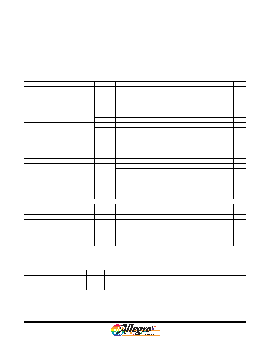
ELECTRICAL CHARACTERISTICS at TJ = 25∞C, V
BB
= 8 to 36 V,
unless noted otherwise
Characteristics
Symbol
Test Conditions
Min.
Typ. Max. Units
Motor Supply Current
I
BB
f
PWM
< 50 kHz
≠
6
8.5
mA
Charge pump on, outputs disabled
≠
3
4.5
mA
Sleep mode
≠
≠
10
A
PHASE, ENABLE, MODE Input
Voltage
V
IH
2.0
≠
≠
V
V
IL
≠
≠
0.8
V
SLEEP Input Voltage
V
IH
2.7
≠
≠
V
V
IL
≠
≠
0.8
V
PHASE, MODE Input Current
1
I
IH
V
IN
= 2.0 V
≠
<1.0
20
A
I
IL
V
IN
= 0.8 V
≠
<≠2.0 ≠20
A
ENABLE Input Current
I
IH
V
IN
= 2.0 V
≠
40
100
A
I
IL
V
IN
= 0.8 V
≠
16
40
A
SLEEP Input Current
I
IH
V
IN
= 2.7 V
≠
27
50
A
I
IL
V
IN
= 0.8 V
≠
<1
10
A
NFAULT Output Voltage
V
OL
I
sink
= 1.0 mA
≠
≠
0.4
V
Input Hysteresis, except SLEEP
V
IHys
100
150
200
mV
Output On Resistance
R
DS(on)
Source driver, I
OUT
= -2.8 A, T
J
=25∞C
≠
0.35
0.48
Source driver, I
OUT
= -2.8 A, T
J
=125∞C
≠
0.55
0.8
Sink driver, I
OUT
= 2.8 A, T
J
=25∞C
≠
0.3
0.43
Sink driver, I
OUT
= 2.8 A, T
J
=125∞C
≠
0.45
0.7
Propagation Delay Time
t
pd
PWM, change to source or sink ON
≠
600
≠
ns
PWM, change to source or sink OFF
≠
100
≠
ns
Crossover Delay
t
COD
≠
500
≠
ns
Protection Circuitry
UVLO Threshold
V
UV
V
BB
increasing
≠
6.5
≠
V
UVLO Hysteresis
V
UVHys
≠
250
≠
mV
Overcurrent Threshold
2
I
OCP
3
≠
≠
A
Overcurrent Protection Period
t
OCP
≠
1.2
≠
ms
Thermal Warning Temperature
T
JW
Temperature increasing
≠
160
≠
∞C
Thermal Warning Hysteresis
T
JWHys
Recovery = T
JW
≠ T
JWHys
≠
15
≠
∞C
Thermal Shutdown Temperature
T
JTSD
Temperature increasing
≠
175
≠
∞C
Thermal Shutdown Hysteresis
T
JTSDHys
Recovery = T
JTSD
≠ T
JTSDHys
≠
15
≠
∞C
1
For input and output current specifications, negative current is defined as coming out of (sourcing) the specified device pin.
2
Overcurrent protection is tested at 25∞C in a restricted range and guaranteed by characterization.
THERMAL CHARACTERISTICS may require derating at maximum conditions, see application information
Characteristic
Symbol
Test Conditions*
Value
Units
Package Thermal Resistance
R
JA
4-layer PCB based on JEDEC standard
34
∫C/W
2-layer PCB with 3.8 in.
2
copper both sides, connected by thermal vias
43
∫C/W
*Additional thermal data available on the Allegro Web site.
Preliminary Data Sheet
Subject to Change without Notice
November 4, 2005

A3950DS
4
Worcester, Massachusetts 01615-0036 (508) 853-5000
115 Northeast Cutoff, Box 15036
www.allegromicro.com
Allegro MicroSystems, Inc.
A3950
DMOS Full-Bridge Motor Driver
V
BB
V
BB
1
2
3
4
6
7
8
9
A
Charge pump and VREG power-on delay (
200 µs)
OutB
OutA
OutA
OutB
5
A
1
2
3
4
5
6
7
9
8
SLEEP
ENABLE
PHASE
MODE
V
OUTA
V
BB
0
V
BB
0
0
V
OUTB
I
OUTX
Timing Diagram: PWM Control
Preliminary Data Sheet
Subject to Change without Notice
November 4, 2005

A3950DS
5
Worcester, Massachusetts 01615-0036 (508) 853-5000
115 Northeast Cutoff, Box 15036
www.allegromicro.com
Allegro MicroSystems, Inc.
A3950
DMOS Full-Bridge Motor Driver
BLANK
NFAULT
Motor lead
short condition
Normal dc
motor capacitance
Charge Pump
Counter
ENABLE,
Source
or Sink
High-Z
I
OUT
x
I
PEAK
I
OCP
V
OUTA
V
OUTB
t
BLANK
t
OCP
Timing Diagram: Overcurrent Control
Preliminary Data Sheet
Subject to Change without Notice
November 4, 2005