
MICROSTEPPING DRIVER
WITH TRANSLATOR
ABSOLUTE MAXIMUM RATINGS
at T
A
= +25∞C
Load Supply Voltage, V
BB
............. 30 V
Output Current, I
OUT
Continuous ..................... ±750 mA
*
Peak................................. ±850 mA
Logic Supply Voltage, V
CC
........... 7.0 V
Logic Input Voltage Range, V
IN
(t
w
>30 ns)............. -0.3 V to +7.0 V
(t
w
<30 ns)................ -1 V to +7.0 V
Sense Voltage, V
SENSE
............... 0.68 V
Reference Voltage, V
REF
................ V
CC
Package Power Dissipation,
P
D
................................. See page 8
Operating Temperature Range,
T
A
........................... -20∞C to +85∞C
Junction Temperature, T
J
......... +150∞C
Storage Temperature Range,
T
S
......................... -55∞C to +150∞C
* Output current rating may be limited by
duty cycle, ambient temperature, and heat
sinking. Under any set of conditions, do not
exceed the specified current rating or a
junction temperature of 150∞C.
Data Sheet
26184.24C
3967
The A3967SLB is a complete microstepping motor driver with
built-in translator. It is designed to operate bipolar stepper motors in
full-, half-, quarter-, and eighth-step modes, with output drive capabil-
ity of 30 V and ±750 mA. The A3967SLB includes a fixed off-time
current regulator that has the ability to operate in slow, fast, or mixed
current-decay modes. This current-decay control scheme results in
reduced audible motor noise, increased step accuracy, and reduced
power dissipation.
The translator is the key to the easy implementation of the
A3967SLB. By simply inputting one pulse on the STEP input the
motor will take one step (full, half, quarter, or eighth depending on two
logic inputs). There are no phase-sequence tables, high-frequency
control lines, or complex interfaces to program. The A3967SLB
interface is an ideal fit for applications where a complex µP is unavail-
able or over-burdened.
Internal circuit protection includes thermal shutdown with hyster-
esis, under-voltage lockout (UVLO) and crossover-current protection.
Special power-up sequencing is not required.
The A3967SLB is supplied in a 24-lead SOIC with copper batwing
tabs. The tabs are at ground potential and need no insulation. A lead-
free (100% matte tin leadframe) version is also available.
FEATURES
s
±750 mA, 30 V Output Rating
s
SatlingtonTM Sink Drivers
s
Automatic Current-Decay Mode Detection/Selection
s
3.0 V to 5.5 V Logic Supply Voltage Range
s
Mixed, Fast, and Slow Current-Decay Modes
s
Internal UVLO and Thermal Shutdown Circuitry
s
Crossover-Current Protection
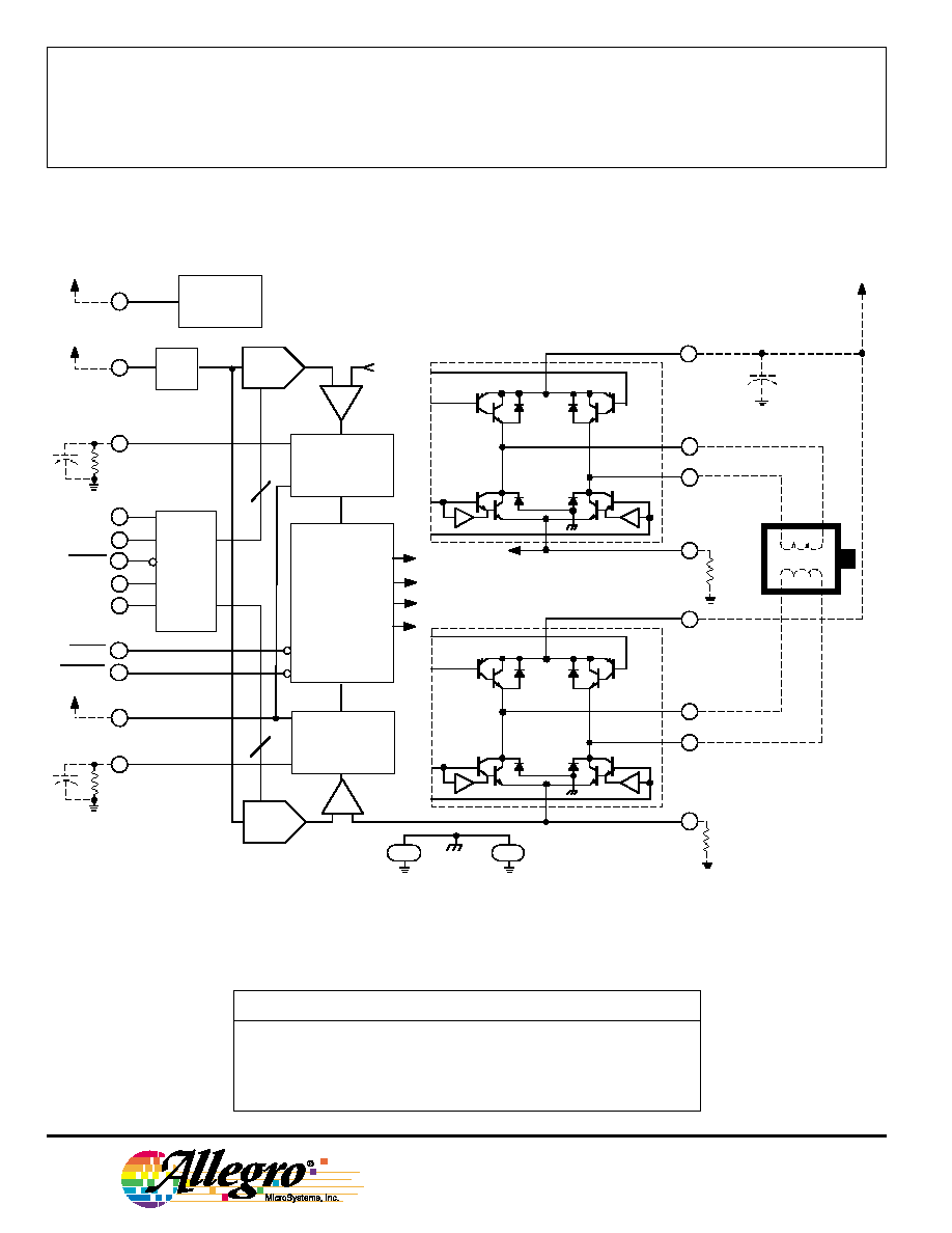
LOAD
SUPPLY
1
SLEEP
ENABLE
OUT
1A
GND
STEP
OUT
1B
RESET
LOAD
SUPPLY
2
SENSE
1
DIR
OUT
2A
PFD
RC
1
REF
˜8
RC
2
LOGIC
SUPPLY
OUT
2B
MS
2
MS
1
SENSE
2
PWM
TIMER
TRANSLATOR
& CONTROL
LOGIC
V
BB2
V
BB1
V
CC
Dwg. PP-075-2
23
17
8
1
2
3
4
5
6
7
9
12
16
15
14
13
24
22
21
20
19
18
11
10
GND
GND
GND
Always order by complete part number:
Part Number
Package
A3967SLB
24-lead batwing SOIC
A3967SLB-T
24-lead batwing SOIC; Lead-free
115 Northeast Cutoff, Box 15036
Worcester, Massachusetts 01615-0036 (508) 853-5000
3967
MICROSTEPPING DRIVER
WITH TRANSLATOR
2
Copyright © 2002, 2003 Allegro MicroSystems, Inc.
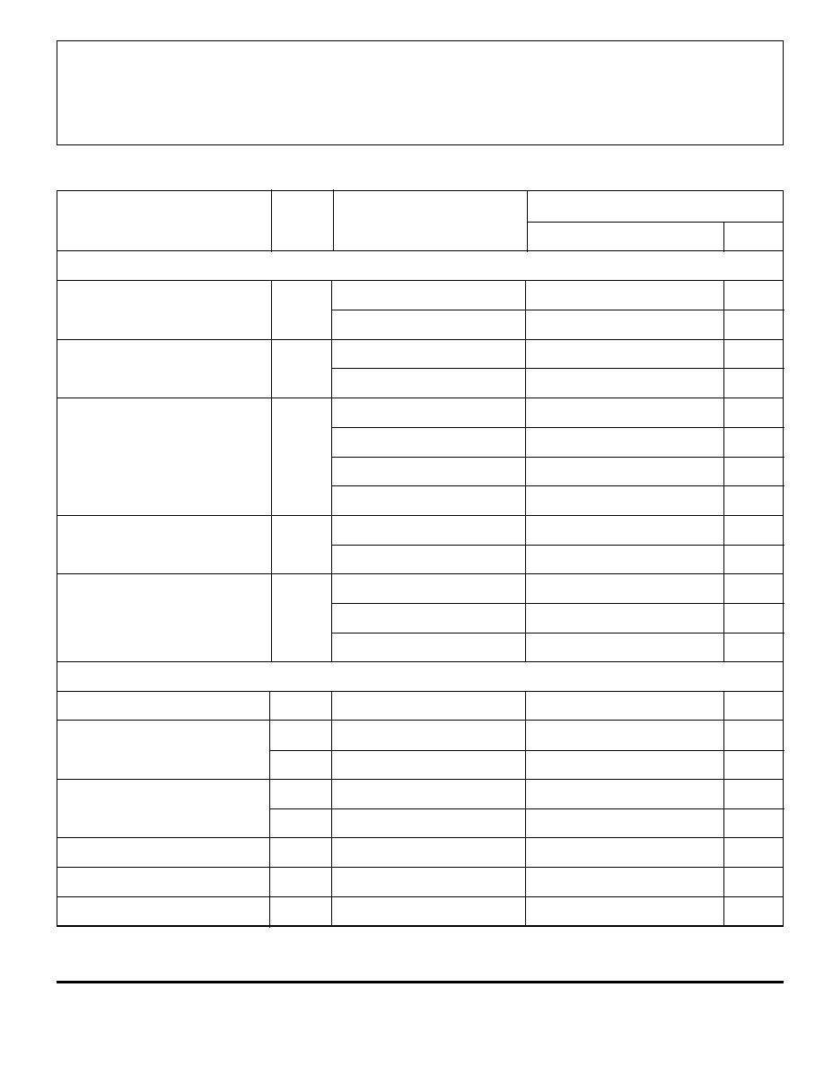
FUNCTIONAL BLOCK DIAGRAM
Table 1. Microstep Resolution Truth Table
MS
1
MS
2
Resolution
L
L
Full step (2 phase)
H
L
Half step
L
H
Quarter step
H
H
Eighth step
19
18
SENSE
1
V
BB1
V
BB2
OUT
1A
OUT
1B
OUT
2A
OUT
2B
SENSE
2
5
9
20
16
21
17
8
4
TRANSLATOR
LOAD
SUPPLY
Dwg. FP-050-3A
PWM TIMER
PWM TIMER
PWM LATCH
BLANKING
MIXED DECAY
CONTROL LOGIC
UVLO
AND
FAULT
DETECT
DAC
+
-
+
-
DAC
SENSE
PWM LATCH
BLANKING
MIXED DECAY
3
3
REF
LOGIC
SUPPLY
V
CC
STEP
DIR
MS
1
SLEEP
MS
2
ENABLE
RC
1
RESET
PFD
RC
2
REF.
SUPPLY
V
PF
˜8
14
1
23
10
11
22
12
13
3
15
24
2
7
6
3967
MICROSTEPPING DRIVER
WITH TRANSLATOR
www.allegromicro.com
3
ELECTRICAL CHARACTERISTICS at T
A
= +25
∞
C, V
BB
= 30 V, V
CC
= 3.0 V to 5.5V (unless otherwise
noted)
Limits
Characteristic
Symbol Test Conditions
Min.
Typ.
Max.
Units
Output Drivers
Load Supply Voltage Range
V
BB
Operating
4.75
≠
30
V
During sleep mode
0
≠
30
V
Output Leakage Current
I
CEX
V
OUT
= V
BB
≠
<1.0
20
µ
A
V
OUT
= 0 V
≠
<-1.0
-20
µ
A
Output Saturation Voltage
V
CE(sat)
Source driver, I
OUT
= -750 mA
≠
1.9
2.1
V
Source driver, I
OUT
= -400 mA
≠
1.7
2.0
V
Sink driver, I
OUT
= 750 mA
≠
0.65
1.3
V
Sink driver, I
OUT
= 400 mA
≠
0.21
0.5
V
Clamp Diode Forward Voltage
V
F
I
F
= 750 mA
≠
1.4
1.6
V
I
F
= 400 mA
≠
1.1
1.4
V
Motor Supply Current
I
BB
Outputs enabled
≠
≠
5.0
mA
RESET high
≠
≠
200
µ
A
Sleep mode
≠
≠
20
µ
A
Control Logic
Logic Supply Voltage Range
V
CC
Operating
3.0
5.0
5.5
V
Logic Input Voltage
V
IN(1)
0.7V
CC
≠
≠
V
V
IN(0)
≠
≠
0.3V
CC
V
Logic Input Current
I
IN(1)
V
IN
= 0.7V
CC
-20
<1.0
20
µ
A
I
IN(0)
V
IN
= 0.3V
CC
-20
<1.0
20
µ
A
Maximum STEP Frequency
f
STEP
500*
≠
≠
kHz
Blank Time
t
BLANK
R
t
= 56 k
, C
t
= 680 pF
700
950
1200
ns
Fixed Off Time
t
off
R
t
= 56 k
, C
t
= 680 pF
30
38
46
µ
s
continued next page ...
3967
MICROSTEPPPING DRIVER
WITH TRANSLATOR
115 Northeast Cutoff, Box 15036
Worcester, Massachusetts 01615-0036 (508) 853-5000
4
ELECTRICAL CHARACTERISTICS at T
A
= +25∞C, V
BB
= 30 V, V
CC
= 3.0 V to 5.5V (unless otherwise
noted)
Characteristic
Symbol
Test Conditions
Limits
Min.
Typ.
Max.
Units
Control Logic (cont'd)
Mixed Decay Trip Point
PFDH
≠
0.6V
CC
≠
V
PFDL
≠
0.21V
CC
≠
V
Ref. Input Voltage Range
V
REF
Operating
1.0
≠
V
CC
V
Reference Input Impedance
Z
REF
120
160
200
k
Gain (G
m
) Error
(note 3)
E
G
VREF = 2 V, Phase Current = 38.37%
≠
≠
±10
%
VREF = 2 V, Phase Current = 70.71%
≠
≠
±5.0
%
VREF = 2 V, Phase Current = 100.00%
≠
≠
±5.0
%
Thermal Shutdown Temp.
TJ
≠
165
≠
∞C
Thermal Shutdown Hysteresis
TJ
≠
15
≠
∞C
UVLO Enable Threshold
V
UVLO
Increasing VCC
2.45
2.7
2.95
V
UVLO Hysteresis
V
UVLO
0.05
0.10
≠
V
Logic Supply Current
I
CC
Outputs enabled
≠
50
65
mA
Outputs off
≠
≠
9.0
mA
Sleep mode
≠
≠
20
µA
* Operation at a step frequency greater than the specifi ed minimum value is possible but not warranteed.
8 microstep/step operation.
NOTES: 1. Typical Data is for design information only.
2. Negative current is defi ned as coming out of (sourcing) the specifi ed device terminal.
3. E
G
= ([V
REF
/8] ≠ V
SENSE
)/(V
REF
/8)

3967
MICROSTEPPING DRIVER
WITH TRANSLATOR
www.allegromicro.com
5
Device Operation. The A3967 is a complete
microstepping motor driver with built in translator for
easy operation with minimal control lines. It is designed
to operate bipolar stepper motors in full-, half-, quarter-
and eighth-step modes. The current in each of the two
output H-bridges is regulated with fixed off time pulse-
width modulated (PWM) control circuitry. The H-bridge
current at each step is set by the value of an external
current sense resistor (R
S
), a reference voltage (V
REF
), and
the DAC's output voltage controlled by the output of the
translator.
At power up, or reset, the translator sets the DACs and
phase current polarity to initial home state (see figures for
home-state conditions), and sets the current regulator for
both phases to mixed-decay mode. When a step command
signal occurs on the STEP input the translator automati-
cally sequences the DACs to the next level (see table 2 for
the current level sequence and current polarity). The
microstep resolution is set by inputs MS
1
and MS
2
as
shown in table 1. If the new DAC output level is lower
than the previous level the decay mode for that H-bridge
will be set by the PFD input (fast, slow or mixed decay).
If the new DAC level is higher or equal to the previous
level then the decay mode for that H-bridge will be slow
decay. This automatic current-decay selection will
improve microstepping performance by reducing the
distortion of the current waveform due to the motor
BEMF.
Reset Input (RESET). The RESET input (active low)
sets the translator to a predefined home state (see figures
for home state conditions) and turns off all of the outputs.
STEP inputs are ignored until the RESET input goes high.
Step Input (STEP). A low-to-high transition on the
STEP input sequences the translator and advances the
motor one increment. The translator controls the input to
the DACs and the direction of current flow in each wind-
ing. The size of the increment is determined by the state
of inputs MS
1
and MS
2
(see table 1).
Microstep Select (MS
1
and MS
2
). Input terminals
MS1 and MS
2
select the microstepping format per
table 1. Changes to these inputs do not take effect until
the STEP command (see figure).
Direction Input (DIR). The state of the DIRECTION
input will determine the direction of rotation of the motor.
Internal PWM Current Control. Each H-bridge is
controlled by a fixed off time PWM current-control circuit
that limits the load current to a desired value (I
TRIP
).
Initially, a diagonal pair of source and sink outputs are
enabled and current flows through the motor winding and
R
S
. When the voltage across the current-sense resistor
equals the DAC output voltage, the current-sense com-
parator resets the PWM latch, which turns off the source
driver (slow-decay mode) or the sink and source drivers
(fast- or mixed-decay modes).
The maximum value of current limiting is set by the
selection of R
S
and the voltage at the V
REF
input with a
transconductance function approximated by:
I
TRIP
max = V
REF
/8R
S
The DAC output reduces the V
REF
output to the
current-sense comparator in precise steps (see table 2 for
% I
TRIP
max at each step).
I
TRIP
= (% I
TRIP
max/100) x I
TRIP
max
Fixed Off-Time. The internal PWM current-control
circuitry uses a one shot to control the time the driver(s)
remain(s) off. The one shot off-time, t
off
, is determined by
the selection of an external resistor (R
T
) and capacitor
(C
T
) connected from the RC timing terminal to ground.
The off time, over a range of values of C
T
= 470 pF to
1500 pF and R
T
= 12 k
to 100 k
is approximated by:
t
off
= R
T
C
T
Functional Description