
26184.23
A3979
Microstepping DMOS Driver with Translator
The A3979 is a complete microstepping motor driver with built-in
translator, designed as a pin-compatible replacement for the successful
A3977, with enhanced microstepping (
1
/
16
step) precision. It is designed
to operate bipolar stepper motors in full-, half-, quarter-, and sixteenth-
step modes, with an output drive capacity of up to 35 V and ±2.5 A. The
A3979 includes a fixed off-time current regulator that has the ability
to operate in Slow, Fast, or Mixed decay modes. This current-decay
control scheme results in reduced audible motor noise, increased step
accuracy, and reduced power dissipation.
The translator is the key to the easy implementation of the A3979. It
allows the simple input of one pulse on the STEP pin to drive the motor
one microstep, which can be either a full step, half, quarter, or sixteenth,
depending on the setting of the MS1 and MS2 logic inputs. There are no
phase-sequence tables, high-frequency control lines, or complex inter-
faces to program. The A3979 interface is an ideal fit for applications
where a complex microprocessor is unavailable or is overburdened.
Internal synchronous-rectification control circuitry is provided to
improve power dissipation during PWM operation. Internal circuit
protection includes: thermal shutdown with hysteresis, UVLO (under-
voltage lockout), and crossover-current protection. Special power-on
sequencing is not required.
The A3979 is supplied in a low-profile (maximum height 1.20 mm),
28-pin TSSOP with exposed thermal pad. The package is available in a
lead (Pb) free version, with 100% matte tin leadframe plating.
±2.5 A, 35 V output rating
Low R
DS(On)
outputs: 0.28 source, 0.22 sink, typical
Automatic current decay mode detection/selection
3.0 to 5.5 V logic supply voltage range
Slow, Fast or Mixed current decay modes
Home output
Synchronous rectification for low power dissipation
Internal UVLO and thermal shutdown circuitry
Crossover-current protection
Use the following complete part number when ordering:
AB SO LUTE MAX I MUM RAT INGS
Load Supply Voltage,V
BB
...................................35 V
Output Current, I
OUT
...................................... ±2.5 A
*
Logic Supply Voltage, V
DD
...............................7.0 V
Logic Input Voltage Range, V
IN
t
W
> 30 ns........................ ≠0.3 V to V
DD
+ 0.3 V
t
W
< 30 ns.............................. ≠1 V to V
DD
+ 1 V
Sense Voltage, V
SENSE
.......................................0.5 V
Reference Voltage, V
REF
......................................V
DD
Package Power Dissipation, P
D
.................See page 5
Operating Temperature Range
Ambient,
T
A
, Range S ................... ≠20∞C to 85∞C
Junction Temperature, T
J(MAX)
.....................150∞C
Storage Temperature, T
S
.................... ≠55∞C to 150∞C
*
Output current rating may be limited by duty cycle,
ambient temperature, and heat sinking. Under any set of
conditions, do not exceed the specified current rating or a
junction temperature of 150∞C.
FEATURES
Approximate Scale 1:1
Package LP, 28-pin TSSOP
with Exposed Thermal Pad
7
8
9
10
11
12
13
6
5
20
19
18
17
16
15
21
22
14
1
2
3
4
26
25
28
27
24
23
VCP
PGND
VREG
STEP
OUT2B
RESET
SR
VBB2
PFD
RC1
AGND
REF
RC2
VDD
OUT2A
MS2
MS1
SENSE2
SENSE1
HOME
DIR
OUT1A
ENABLE
OUT1B
CP2
CP1
SLEEP
VBB1
Translator
and
Control
Logic
˜8
Reg
Charge
Pump
PWM
Timer
Part Number
Pb-free
Ambient, T
A
(∞C)
A3979SLP
≠
≠20 to 85
A3979SLP-T
Yes
AGND
and
PGND
must be
connected together externally.

3
26184.23
Worcester, Massachusetts 01615-0036 (508) 853-5000
115 Northeast Cutoff, Box 15036
www.allegromicro.com
Allegro MicroSystems, Inc.
A3979
DMOS Microstepping Driver with Translator
ELECTRICAL CHARACTERISTICS
at T
A
= 25∞C, V
BB
= 35 V, V
DD
= 3.0 to 5.5 V (unless otherwise noted)
Characteristics
Symbol
Test Conditions
Min.
Typ.
1
Max.
Units
Output Drivers
Load Supply Voltage Range
V
BB
Operating
8
≠
35
V
During Sleep mode
0
≠
35
V
Output Leakage Current
2
I
DSS
V
OUT
= V
BB
≠
<1.0
20
A
V
OUT
= 0 V
≠
<1.0
≠20
A
Output On Resistance
R
DS(On)
Source driver, I
OUT
= ≠2.5 A
≠
0.28
0.335
Source driver, I
OUT
= 2.5 A
≠
0.22
0.265
Body Diode Forward Voltage
V
F
Source diode, I
F
= ≠2.5 A
≠
≠
1.4
V
Sink diode, I
F
= 2.5 A
≠
≠
1.4
V
Motor Supply Current
I
BB
f
PWM
< 50 kHz
≠
≠
8.0
mA
Operating, outputs disabled
≠
≠
6.0
mA
Sleep mode
≠
≠
20
A
Control Logic
Logic Supply Voltage Range
V
DD
Operating
3.0
5.0
5.5
V
Logic Supply Current
I
DD
f
PWM
< 50 kHz
≠
≠
12
mA
Outputs off
≠
≠
10
mA
Sleep mode
≠
≠
20
A
Logic Input Voltage
V
IN(1)
0.7
◊
V
DD
≠
≠
V
V
IN(0)
≠
≠
0.3
◊
V
DD
V
Logic Input Current
2
I
IN(1)
V
IN
= 0.7
◊
V
DD
≠20
<1.0
20
A
I
IN(0)
V
IN
= 0.3
◊
V
DD
≠20
<1.0
20
A
Reference Input Voltage Range
V
REF
Operating
0
≠
V
DD
V
Reference Input Current
I
REF
≠
0
±3
A
HOME Output Voltage
V
HOME(1)
I
HOME(1)
= ≠200 A
0.7
◊
V
DD
≠
≠
V
V
HOME(0)
I
HOME(0)
= 200 A
≠
≠
0.3
◊
V
DD
V
Mixed Decay Mode Trip Point
V
PFDH
≠
0.6
◊
V
DD
≠
V
V
PFDL
≠
0.21
◊
V
DD
≠
V
Gain (G
m
) Error
3
E
G
V
REF
= 2 V,
Phase Current =
38.27%
≠
≠
±10
%
V
REF
= 2 V,
Phase Current
= 70.71%
≠
≠
±5.0
%
V
REF
= 2 V,
Phase Current
= 100.00%
≠
≠
±5.0
%
STEP Pulse Width
t
W
1
≠
≠
s
Blank Time
t
BLANK
R
T
= 56 k, C
T
= 680 pF
700
950
1200
ns
Fixed Off-Time
t
OFF
R
T
= 56 k, C
T
= 680 pF
30
38
46
s
Crossover Dead Time
t
DT
Synchronous rectification enabled
100
475
800
ns
Continued on the next page...

4
26184.23
Worcester, Massachusetts 01615-0036 (508) 853-5000
115 Northeast Cutoff, Box 15036
www.allegromicro.com
Allegro MicroSystems, Inc.
A3979
DMOS Microstepping Driver with Translator
1
Typical data are for initial design estimations only, and assume optimum manufacturing and application conditions. Performance may vary for
individual units, within the specified maximum and minimum limits.
2
Negative current is defined as coming out of (sourcing from) the specified device pin.
3
E
G
= ( [ V
REF
/ 8]
≠ V
SENSE
) / ( V
REF
/ 8 ).
ELECTRICAL CHARACTERISTICS, continued
at T
A
= 25∞C, V
BB
= 35 V, V
DD
= 3.0 to 5.5 V (unless otherwise noted)
Thermal Shutdown Temperature
T
JSD
≠
165
≠
∞C
Thermal Shutdown Hysteresis
T
JSDHYS
≠
15
≠
∞C
UVLO Enable Threshold
V
UVLO
Increasing V
DD
2.45
2.7
2.95
V
UVLO Hysteresis
V
UVLOHYS
0.05
0.10
≠
V
Characteristics
Symbol
Test Conditions
Min.
Typ.
1
Max.
Units
5
26184.23
Worcester, Massachusetts 01615-0036 (508) 853-5000
115 Northeast Cutoff, Box 15036
www.allegromicro.com
Allegro MicroSystems, Inc.
A3979
DMOS Microstepping Driver with Translator
Characteristic
Symbol
Test Conditions*
Value
Units
Package Thermal Resistance
R
JA
Two-layer PCB with 3.8 in.
2
of copper area on each side
connected with thermal vias and to device exposed pad
32
∫C/W
High-K PCB (multilayer with significant copper areas,
based on JEDEC standard)
28
∫C/W
*Additional thermal information available on Allegro Web site.
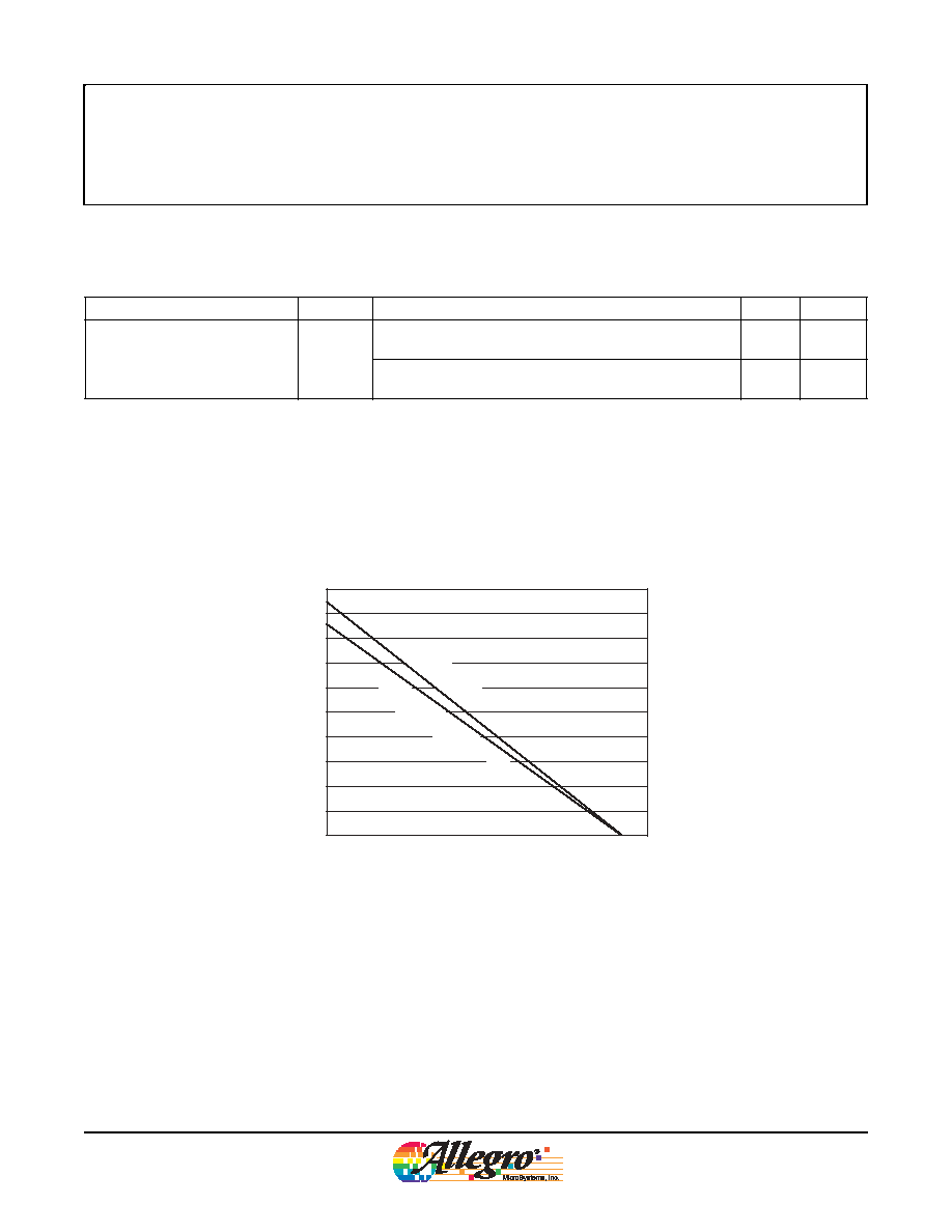
THERMAL CHARACTERISTICS may require derating at maximum conditions, see application information
Temperature (∞C)
Power D
i
s
s
ip
a
t
io
n, P
D
(W)
0.0
0.5
2.0
2.5
3.0
3.5
4.0
4.5
5.0
1.0
1.5
20
40
60
80
100
120
140
160
Maximum Power Dissipation, P
D(max)
(R
JA
= 32
∫C/W)
(R
JA
= 28 ∫C/W)
High-K PCB
2-Layer PCB with 3.8 in
2
copper per side
