2993
DUAL H-BRIDGE
MOTOR DRIVERS
DISCONTINUED PRODUCT
-- FOR REFERENCE ONL
Y
B
1
2
3
4
5
6
7
8
PHASE
GROUND
GROUND
OUT
OUT
GROUND
GROUND
BB
V
LOGIC SUPPLY
ENABLE
B
OUT
1B
OUT
2B
LOAD SUPPLY
ENABLE
PHASE
V
EA
2A
1A
A
A
V
EB
DD
V
LOGIC
LOGIC
9
10
11
12
13
14
15
16
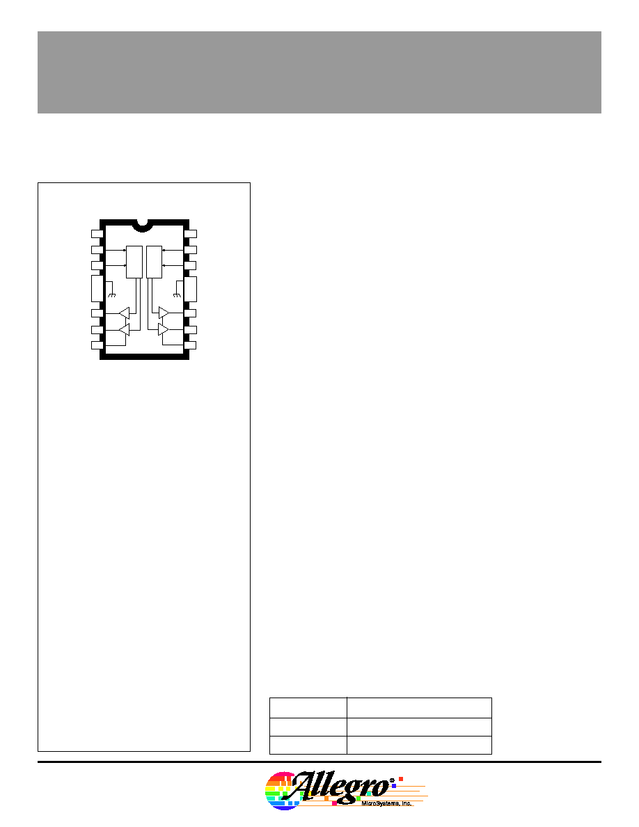
UDN2993B
2993
Dwg. No. A-12,455
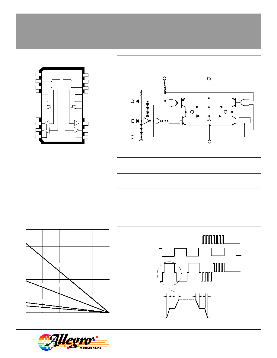
DUAL H-BRIDGE MOTOR DRIVERS
Cost-effective monolithic drive electronics for bipolar stepper and
dc (brush) servo motors to 30 V and 500 mA is very practical with the
UDN2993B and UDN2993LB. These dual full-bridge motion control
ICs integrate separate inputs, level shifting for upper power outputs,
control logic, integral inductive transient protection, and source (upper)
and sink (lower) drivers in an H-bridge configuration. The single-chip
power IC provides improved space utilization and reliability unmatched
by discrete component circuitry.
Excepting the power supply connections, the two H-bridges are
independent. An ENABLE input is provided for each bridge and
permits pulse-width modulation (PWM) through the use of external
circuitry. PWM drive techniques provide the benefits of reduced power
dissipation, improved motor performance (especially torque), and
positively affect system efficiency. Separate PHASE inputs for each
bridge determine the direction of current flow in the load. Additionally,
each pair of (sink) emitters are terminated to package connections.
This allows the use of current-sensing circuitry. Both devices
incorporate an intrinsic "dead time" to preclude high crossover
(or cross-conduction) currents during changes in direction (phase).
These devices are packaged in plastic DIPs (suffix B) or surface-
mountable wide-body SOICs (suffix LB) with copper lead frames for
optimum power dissipation without heat sinks. The lead configurations
allow automatic insertion, fit standard IC sockets or printed wiring
board layouts, and enable easy attachment of a heat sink for maximum
power-handling capability. The heat-sink tabs are at ground potential
and require no insulation.
Dual full-bridge drivers with peak current ratings of
�
3 A are
supplied as the UDN2998W.
FEATURES
s
�
600 mA Output Current
s
Output Voltage to 30 V
s
Crossover Current Protection
s
TTL/NMOS/CMOS Compatible Inputs
s
Low Input Current
s
Internal Clamp Diodes
s
Automotive Capable
ABSOLUTE MAXIMUM RATINGS
at T
J
+150
�
C
Load Supply Voltage, V
BB
.................... 30 V
Logic Supply Voltage, V
DD
................... 7.0 V
Logic Input Voltage Range, V
PHASE
or
V
ENABLE
............... -0.3 V to V
DD
+ 0.3 V
Output Current, I
OUT
.....................
�
600 mA
Sink Driver Emitter Voltage,
V
E
.................................................. 1.5 V
Package Power Dissipation,
P
D
........................................ See Graph
Operating Temperature Range,
T
A
................................. -20
�
C to +85
�
C
Storage Temperature Range,
T
S
............................... -55
�
C to +150
�
C
IMPORTANT: Load supply voltage must never be
applied without logic supply voltage present.
NOTE: Output current rating may be limited by
chopping frequency, ambient temperature,
airflow, and heat sinking. Under any set of
conditions, do not exceed the specified maximum
current and a junction temperature of +150
�
C.
Data Sheet
29319.5A
Always order by complete part number:
Part Number
Package
UDN2993B
16-Pin DIP
UDN2993LB
20-Lead Wide-Body SOIC
2993
DUAL H-BRIDGE
MOTOR DRIVERS
ELECTRICAL CHARACTERISTICS at T
A
= +25
�
C, V
BB
= 30 V, V
DD
= 5 V, V
E
= 0 V, T
J
+150
�
C
Figure 1 (unless otherwise noted).
Limits
Characteristic
Symbol
Test Conditions
Min.
Typ.
Max.
Units
Output Drivers
Operating Voltage Range
V
BB
10
--
30
V
Output Leakage Current
I
CEX
V
ENABLE
= 0.8 V, V
OUT
= V
BB
, Note 2
--
< 1.0
50
�
A
V
ENABLE
= 0.8 V, V
OUT
= 0 V, Note 2
--
< -1.0
-50
�
A
Output Saturation Voltage
V
CE(SAT)
V
ENABLE
= 2.4 V, I
OUT
= 500 mA
--
1.6
1.8
V
V
ENABLE
= 2.4 V, I
OUT
= -500 mA
--
1.6
2.0
V
Output Sustaining Voltage
V
CE(sus)
I
OUT
=
�
500 mA, Figure 2, Note 2
30
--
--
V
Motor Supply Current
I
BB(ON)
V
ENABLE
= 2.4 V, Outputs Open, Note 2
--
1.0
3.0
mA
I
BB(OFF)
V
ENABLE
= 0.8 V, Outputs Open, Note 2
--
250
300
�
A
Source Driver Rise Time
t
r
I
OUT
= -500 mA
--
75
--
ns
Source Driver Fall Time
t
f
I
OUT
= -500 mA
--
280
--
ns
Clamp Diode Forward Voltage
V
F
I
F
= 500 mA
--
1.6
1.8
V
Control Logic (PHASE or ENABLE)
Logic Input Current
I
IN(1)
V
PHASE
or V
ENABLE
= 2.4 V
--
< 1.0
10
�
A
I
IN(0)
V
PHASE
or V
ENABLE
= 0.8 V
--
-200
-300
�
A
Logic Input Voltage
V
IN(1)
2.4
--
--
V
V
IN(0)
--
--
0.8
V
Logic Supply Current
I
DD
--
14
20
mA
Turn-On Delay Time
t
pd0
ENABLE Input to Source Drivers
--
250
--
ns
Turn-Off Delay Time
t
pd1
ENABLE lnput to Source Drivers
--
500
--
ns
NOTES: 1. Each driver is tested separately.
2. Test is performed with V
PHASE
= 0.8 V and then repeated for V
PHASE
= 2.4 V.
3. Negative current is defined as coming out of (sourcing) the specified device pin.