 | –≠–ª–µ–∫—Ç—Ä–æ–Ω–Ω—ã–π –∫–æ–º–ø–æ–Ω–µ–Ω—Ç: A8285SLB | –°–∫–∞—á–∞—Ç—å:  PDF PDF  ZIP ZIP |

Data Sheet
27448.003c
A8285/A8287
LNB Supply and Control Voltage Regulator
Intended for analog and digital satellite receivers, the LNB (low noise
block) converter regulator is a monolithic linear and switching voltage
regulator, specifi cally designed to provide power and interface signals
to an LNB downconverter, via coaxial cable.
The device uses a 2-wire bidirectional serial interface, compatible with
the I
2
C (Inter-C bus) standard, that operates up to 400 kHz.
The A8285 is supplied in a 16-lead plastic power SOIC with copper
batwing tabs (suffi x LB). The A8287 is supplied in a 24-lead plastic
power SOIC with copper batwing tabs (part number suffi x LB).
LNB selection and standby function
Provides up to 500 mA load current
Two-wire serial I
2
C interface
Built-in tone oscillator, factory-trimmed to 22 kHz; facilitates
DiSEqCTM 2.0 encoding
Auxiliary modulation input
22 kHz tone detector facilitates DiSEqCTM decoding
(A8287 only)
Tracking switch-mode power converter for lowest dissipation
LNB overcurrent protection and diagnostics
Internal overtemperature protection
LNB voltages (16 possible levels) compatible with all common
standards
Use the following complete part numbers when ordering:
Preliminary Data Sheet
Subject to Change without Notice
January 21, 2004
AB SO LUTE MAX I MUM RAT INGS
8
ADD
4
GND
7
EXTM
3
IRQ
6
VIN
2
SDA
5
VREG
9
NC
13
GND
10
TCAP
14
LX
11
TOUT
15
BOOST
12
LNB
16
VCP
1
SCL
A8287SlB
SOIC
Part Number
Package
Description
A8287SLB
24-pin, batwing SOIC
All features
A8285SLB
16-pin, batwing SOIC
Tone detect not provided
Load Supply Voltage, V
IN
....................................16 V
Output Current, I
OUT
..................Internally Limited*
Output Voltage
LNB,
BOOST .....................≠0.3 V to 28 V
TOUT ................................. ≠0.3 V to 22 V
Logic Input
EXTM ...................................≠0.3 V to 5 V
Other .................................... ≠0.3 V to 7 V
Logic Output ........................................ ≠0.3 V to 7 V
Package Power Dissipation ...........See power dis si-
pation information in the Application Information section
Operating Temperature
Ambient,
T
A
.......................≠20∞C to +85∞C
Junction,
T
J
.......................≠20∞C to +150∞C
Storage,T
S
.......................≠55∞C to +150∞C
* Output current rating may be limited by duty cycle,
ambient temperature, and heat sinking. Under any
set of conditions, do not exceed the specifi ed current
rating or a junction temperature of +150∞C.
13
TDI
14
NC
TCAP
15
16
TOUT
17
LNB
21
GND
18
GND
22
GND
19
GND
23
BOOST
20
LX
24
VCP
12
TDO
11
ADD
10
EXTM
9
VIN
8
VREG
4
GND
7
GND
3
IRQ
6
GND
2
SDA
5
GND
1
SCL
A8285SlB
SOIC
FEATURES
Scale 1:1
Scale 1:1

2
Worcester, Massachusetts 01615-0036 (508) 853-5000
115 Northeast Cutoff, Box 15036
www.allegromicro.com
Data Sheet
Preliminary
27448.003c
A8285/A8287
LNB Supply and Control Voltage Regulator
Functional Block Diagram
22 kHz Tone
Detector
Internal
Regulator
Boost Converter
Charge
Pump
Clock
Divider
22 kHz
Tone
Generator
I C Interface
2
Output
Voltage
Select
Fault Monitor
Overcurrent
TSD
Undervoltage
VREG
BOOST
Feedback
33 uH
33 uF
EXTM
V
IN
SDA
SCL
ADD
IRQ
100 mV
VIN
LX
100 nF
VCP
BOOST
OSC In
DISABLE
100 nF
LNB
220
6.8 nF
220 uH
220 nF
220 nF
TCAP
TOUT
TDI
10 nF
V
DD
TDO
V
DD
OSC
Overcurrent
VPUMP
220 nF
Overcurrent
15
100 uF
100 nF
C10
C1
L1
D1
C5
C2
C4
C3
R3 R4 R5
R6
C9
R2
C8
D2
C6
C7
L2
R1
Tracking
Regulator
GM
ID
Characteristics
Suggested Manufacturer
C1
33 µF, 25 V, esr < 200 m, I
ripple
> 350 mA
Nichicon, part number UHC1E330MET
C2, C5,C10
100 nF, 50 V, X5R or X7R
C4
100 µF, 35 V, esr < 75 m, I
ripple
> 800 mA
Nichicon, part number UHC1V101MPT
C3,C6,C7
220 nF, 50 V, X5R or X7R
C8
6.8 nF, 50 V; Y5V, X5R, or X7R
C9
10 nF (maximum), 50 V; Y5V, X5R, or X7R
R1
15
, 1%, c W
R2
220
, 1%, 2 W
R3-R6
Value determined by V
DD
, bus capacitance. etc.
L1
33 µH, I
DC
> 1.3 A
TDK, part number TSL0808-330K1R4; Coilcraft, part number DR0810-333
L2
220 µH, I
DC
> 0.5 A
TDK, part number TSL0808-221KR54; Coilcraft, part number DR0810-224
D1
1 A, 35 V or 40 V, Schottky diode
Various, part number 1N5819; Sanken, part number AW04
D2
1 A, 100 V, 1N4002
Tone detector and leads TDI and TDO are not provided in 16-pin package (A8285).

3
Worcester, Massachusetts 01615-0036 (508) 853-5000
115 Northeast Cutoff, Box 15036
www.allegromicro.com
Data Sheet
Preliminary
27448.003c
A8285/A8287
LNB Supply and Control Voltage Regulator
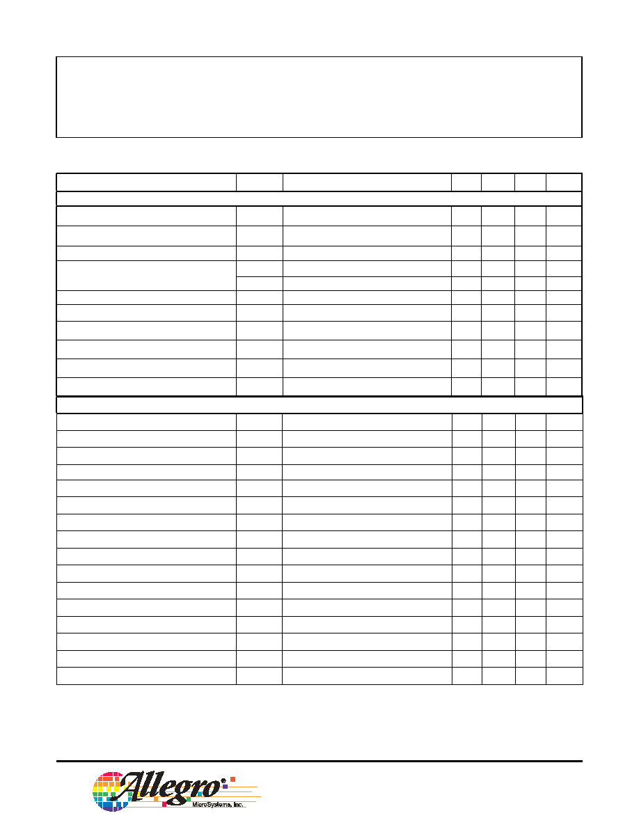
Characteristics
Symbol
Test Conditions
Min.
Typ.
Max.
Units
Set-point Accuracy, load and line
regulation
V
O1
Relative to target voltage selected, with:
I
LOAD
= 0 to 500 mA
-4.5
0
4.5
%
Supply Current
I
CC
ENB = Low, LNB output disabled
≠
≠
7
mA
I
CCEN
ENB = High, LNB output enabled, I
LOAD
= 0mA
≠
≠
15
mA
Boost Switch-On Resistance
R
DSBOOST
T
J
= 25 ∞C, I
LOAD
= 500mA
≠
400
500
m
Switching Frequency
fo
≠
320
352
384
kHz
Switch Current Limit
≠
V
IN
= 12 V
2.0
3
4.0
A
Linear Regulator Voltage Drop
V
REG
V
BOOST
≠ V
LNB
, no tone signal, I
LOAD
= 500 mA
400
600
800
mV
Slew Rate Current on TCAP
I
CAP
Charging
≠12.5
≠10
≠7.5
µA
Discharging
7.5
10
12.5
µA
Output Voltage Slew Period
t
slew
V
LNB
= 13 to 18 V, TCAP = 6.8 nF, I
LOAD
= 500 mA
≠
500
≠
µs
Output Reverse Current
I
OR
ENB = Low, V
LNB
= 28 V with C4 fully charged
≠
1
5
mA
Ripple and Noise on LNB Output
V
RN
See notes 1 and 2
≠
≠
50
mV
pp
Protection Circuitry
Overcurrent Limit
I
LIM
High limit
Low limit
550
400
700
500
850
600
mA
mA
Overcurrent Disable Time
t
DIS
≠
1.2
≠
1.7
ms
V
IN
Undervoltage Threshold
UV
OFF
Guaranteed turn-off
8.65
9.15
9.65
V
V
IN
Turn-On Threshold
UV
ON
Guaranteed turn-on
8.75
9.25
9.75
V
Power-Not-Good Flag Set
PNG
set
≠
77
85
93
%V
LNB
Power-Not-Good Flag Reset
PNG
reset
≠
82
90
98
%V
LNB
Thermal Shutdown Threshold
T
J
See note 1
≠
165
≠
∞C
Thermal Shutdown Hysteresis
T
J
See note 1
≠
20
≠
∞C
ELECTRICAL CHARACTERISTICS at T
A
= +25∞C, V
IN
= 10 to 16 V (unless otherwise noted)
Continued on next page
4
Worcester, Massachusetts 01615-0036 (508) 853-5000
115 Northeast Cutoff, Box 15036
www.allegromicro.com
Data Sheet
Preliminary
27448.003c
A8285/A8287
LNB Supply and Control Voltage Regulator
ELECTRICAL CHARACTERISTICS (continued) at T
A
= +25∞C, V
IN
= 10 to 16 V (unless otherwise noted)
Characteristics
Symbol
Test Conditions
Min.
Typ.
Max.
Units
Tone Characteristics
Tone Frequency
f
TONE
≠
20
22
24
kHz
Tone Pull-Down Current
I
TONE
≠
30
40
50
mA
Tone Turn-On and Turn-Off Delays
t
DEL
Using EXTM pin
≠
≠
1
µs
External Tone Logic Input
V
IH
≠
2
≠
≠
V
V
IL
≠
≠
≠
0.8
V
Input Leakage
I
IL
≠
≠1
≠
1
µA
Tone Detector Input Amplitude
V
TDI
f
IN
= 22 kHz
260
≠
1000
mV
Tone Detector Frequency Capture
f
TDI
600 mV
pp
sinewave
17.6
≠
26.4
kHz
Tone Detector Input Impedance
Z
TDI
See note 1
≠
8.6
≠
k
Tone Detector Output Voltage
V
OL
Tone present, I
LOAD
= 3 mA
≠
≠
0.4
V
Tone Detector Output Leakage
I
OL
Tone absent, V
O
= 7 V
≠
≠
10
µA
I
2
C
Interface
Logic Input (SDA,SCL) Low Level
V
IL
≠
≠
≠
0.8
V
Logic Input (SDA,SCL) High Level
V
IH
≠
2
≠
≠
V
Input Hysteresis
V
HYS
≠
≠
150
≠
mV
Logic Input Current
I
IN
V
IN
= 0 V to 7 V
≠10
<±1.0
10
µA
Output Voltage (SDA, IRQ)
V
OL
I
LOAD
= 3 mA
≠
≠
0.4
V
Output Leakage (SDA, IRQ)
I
OL
V
O
= 0 V to 7 V
≠
≠
10
µA
SCL Clock Frequency
f
CLK
≠
0
≠
400
kHz
Output Fall Time
t
OF
V
IH
to V
IL
≠
≠
250
ns
Bus Free Time Between Stop and Start
t
BUF
See I
2
C Interface Timing Diagram
1.3
≠
≠
µs
Hold Time for Start Condition
t
HD:STA
See I
2
C Interface Timing Diagram
0.6
≠
≠
µs
Setup Time for Start Condition
t
SU:STA
See I
2
C Interface Timing Diagram
0.6
≠
≠
µs
SCL Low Time
t
LOW
See I
2
C Interface Timing Diagram
1.3
≠
≠
µs
SCL High Time
t
HIGH
See I
2
C Interface Timing Diagram
0.6
≠
≠
µs
Data Setup Time
t
SU:DAT
See note1; I
2
C Interface Timing Diagram
100
≠
≠
ns
Data Hold Time
t
HD:DAT
See I
2
C Interface Timing Diagram
0
≠
900
ns
Setup Time for Stop Condition
t
SU:STO
See I
2
C Interface Timing Diagram
0.6
≠
≠
µs
Continued on next page

5
Worcester, Massachusetts 01615-0036 (508) 853-5000
115 Northeast Cutoff, Box 15036
www.allegromicro.com
Data Sheet
Preliminary
27448.003c
A8285/A8287
LNB Supply and Control Voltage Regulator
I2C Address Setting
ADD Voltage for Address 0001,000
Address1
≠
0
≠
0.7
V
ADD Voltage for Address 0001,001
Address2
≠
1.3
≠
1.7
V
ADD Voltage for Address 0001,010
Address3
≠
2.3
≠
2.7
V
ADD Voltage for Address 0001,011
Address4
≠
3.3
≠
5
V
1 Guaranteed by design.
2 Use recommended components and adhere to layout guidelines.
ELECTRICAL CHARACTERISTICS (continued) at T
A
= +25∞C, V
IN
= 10 to 16 V (unless otherwise noted)
Characteristics
Symbol
Test Conditions
Min.
Typ.
Max.
Units
t
SU:STA
t
HD:STA
t
SU:DAT
t
HD:DAT
t
BUF
t
SU:STO
t
HIGH
t
LOW
SDA
SCL
I
2
C Interface Timing Diagram