 | ÐлекÑÑоннÑй компоненÑ: A8423KL | СкаÑаÑÑ:  PDF PDF  ZIP ZIP |
Äîêóìåíòàöèÿ è îïèñàíèÿ www.docs.chipfind.ru
Preliminary
Subject to Change without Notice
February 9, 2004
Datasheet
A8423-DS Rev
.0
A8423
LIN Bus Transceiver with Integrated Voltage Regulator
The A8423 provides the physical interface requirements of the LIN
(Local Interconnect Network) serial communications bus plus an inte-
grated voltage regulator that is permanently enabled. These allow the
development of simple, inexpensive slave nodes in a LIN-Bus system.
The LIN transceiver is compatible with LIN-Bus systems that conform
to the LIN Protocol Specifi cation, Revision 1.2. It provides all the
necessary interface and timing control to convert signals to and from
the bidirectional LIN Bus to individual transmit and receive signals at
logic-compatible levels.
The A8423 provides regulated 5V output with a current limit in excess
of 50 mA. This is suffi cient to power a microcontroller handling the
LIN slave node protocol.
The A8423 is supplied in 8-lead plastic SOIC (part number suffi x L).
Compatible with LIN Bus, Revision 1.2 systems
Data rate up to 20 kbaud
Normal operation from 7 to 30 V
Handles 40 V transients during load dump
Handles automotive transients per ISO 7637
Unpowered node does not disturb the network
4 kV (hbm) ESD protection on LIN and WAKE pins
Low quiescent current regulator for slave microcontroller supply
Interface to slave microcontroller
8-pin small outline surface mount package
Use the following complete part number when ordering:
AB SO LUTE MAX I MUM RAT INGS
Part Number
Package
Description
A8423KL
8-lead, SOIC
Continuous voltage regulator
Supply Voltage, VSUP Continuous.....................30 V
Supply Voltage, VSUP Transient (500 ms).........40 V
LIN Bus Voltage, LIN........................... 18 to +40 V
Wake Pin ............................................... 18 to +40 V
Logic Pins: RX, TX, EN ...................... 0.3 V to 7 V
Package Power Dissipation, P
D
......see chart, page 6
Operating Temperature Range
Ambient Temperature, T
A
..........40°C to +125°C
Junction Temperature, T
J
...........55°C to +150°C
Storage Temperature, T
S
..........55°C to +150°C
FEATURES
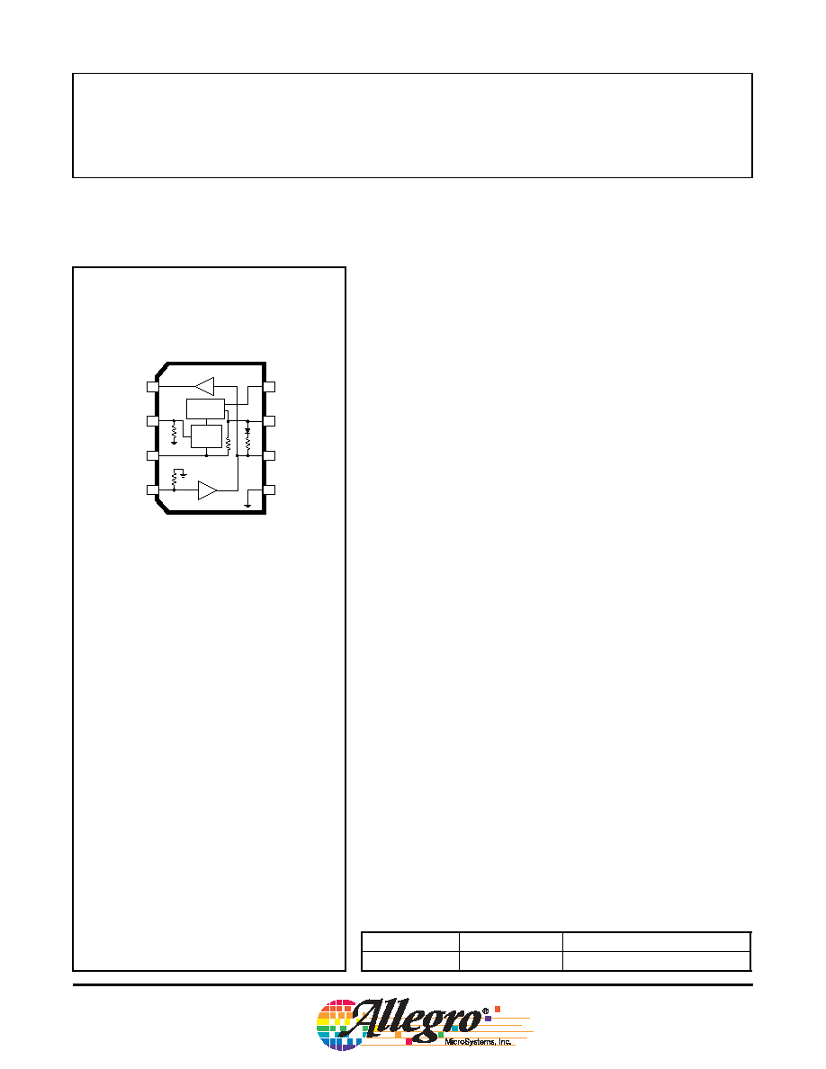
A8423
SOIC
2
3
4
1
7
6
5
8
RX
EN
WAKE
TX
VREG
VSUP
LIN
GND
Control
Regulator
APPLICATIONS
Automotive, industrial, and consumer LIN-Bus systems
2
Worcester, Massachusetts 01615-0036 (508) 853-5000
115 Northeast Cutoff, Box 15036
www.allegromicro.com
Datasheet
A8423-DS Rev
.0
A8423
LIN Bus Transceiver with Integrated Voltage Regulator
Preliminary Subject to Change
Without Notice February 9, 2004
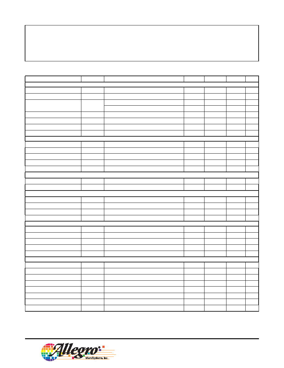
ELECTRICAL CHARACTERISTICS
at T
J
= 40°C to 150ºC, V
SUP
= 7 V to 18 V (unless otherwise noted)
Characteristics
Symbol
Test Conditions
Min.
Typ.
Max.
Units
VSUP Power Supply
Operating Voltage Range
V
SUP
Continuous
7
30
V
V
SUP
Transient; 500 ms
40
V
Supply Current
I
SUP
LIN output recessive (High); V
WAKE
= 0
0.8
1
mA
LIN output dominant (Low); V
WAKE
= 0
1.5
2
mA
Supply Standby Current
I
STBY
V
WAKE
= 0, LIN = N.C.
0.8
1
mA
LIN = Dominant (Low), Wake = N.C.
1.5
2
mA
Supply Sleep Current
I
SLEEP
IREG < 20 µA
80
100
µA
Undervoltage Threshold
VSUP
UV
4.8
5.0
5.2
V
TX and EN Input
Low Level Input Voltage
V
IL
0.8
V
High Level Input Voltage
V
IH
2
V
Input Hysteresis
V
IHYS
300
mV
Pull-Down Resistor
R
PD
EN pin
60
100
200
k
Pull-Up Resistor
R
PU
TX pin
60
100
200
k
RX Output
Low Level Output Current
I
OL
V
RX
= 0.4 V
1.5
mA
High Level Leakage Current
I
OH
V
RX
= 5 V
5
µA
Wake Input
Low Level Input Voltage
V
IL
V
SUP
5
V
High Level Input Voltage
V
IH
V
SUP
1
V
Pull-up Current
I
IL
V
WAKE
= 0 V
40
µA
High Level Leakage Current
I
IH
V
WAKE
= V
SUP
= 30 V
5
µA
VREG Regulated 5V Supply
Output Voltage
V
REG
I
OUT
= 0 to 50 mA
4.5
5.0
5.5
V
Output Current Limit
IREG
LIM
V
REG
= 0 V
180
mA
External Decoupling Cap
V
REG
to GND
1
µF
Line Regulation
I
OUT
= 30 mA
100
mV
Load Regulation
V
SUP
= 13.5 V; I
OUT
= 1 to 30 mA
100
mV
LIN Interface
Output Short Circuit Current
I
OSC
60
85
110
mA
Output Voltage Recessive
V
OR
V
TX
= 5 V; I
LIN
= 0 mA
0.9 V
SUP
V
Output Voltage Dominant
V
OD
V
TX
= 0 V; I
LIN
= 40 mA
1
1.2
V
High Level Leakage Current
I
IH
V
LIN
= V
SUP
10
µA
Termination Resistance
R
SLAVE
20
30
47
k
Input Threshold Dominant
V
THDOM
V
LIN
Recessive to Dominant
0.4 V
SUP
V
Input Threshold Recessive
V
THREC
V
LIN
Dominant to Recessive
0.6 V
SUP
V
Input Threshold Hysteresis
VLIN
HYS
0.05 V
SUP
0.1 V
SUP
0.175 V
SUP
V
3
Worcester, Massachusetts 01615-0036 (508) 853-5000
115 Northeast Cutoff, Box 15036
www.allegromicro.com
Datasheet
A8423-DS Rev
.0
A8423
LIN Bus Transceiver with Integrated Voltage Regulator
Preliminary Subject to Change
Without Notice February 9, 2004
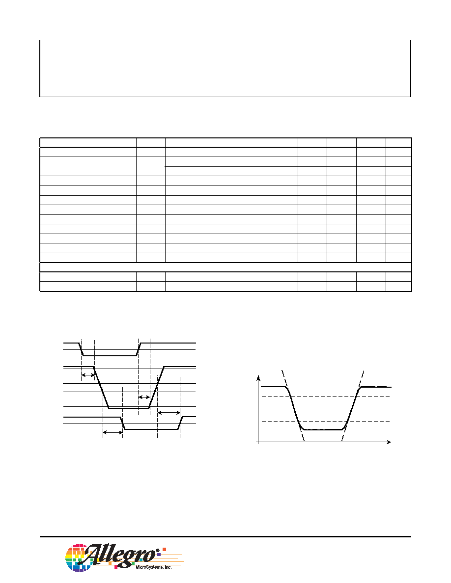
DYNAMIC CHARACTERISTICS
at T
J
= 40°C to 150ºC, V
SUP
= 7 V to 18 V (unless otherwise noted)
Characteristics
Symbol
Test Conditions
Min.
Typ.
Max.
Units
LIN Falling Edge Slew Rate
1
S
HL
80% to 20%
1
2
3
V/µs
LIN Rising Edge Slew Rate
1
S
LH
20% to 80% into >1 k and < 5 nF
1
2
3
V/µs
20% to 80% into >1 k and < 10 nF
1
V/µs
LIN Rise Fall Symmetry
t
SYM
20% to 80% into > 1 k and < 5 nF
2
2
µs
TX Propagation Delay H
L
t
TXL
TX H
L; LIN crossing 95%
1.5
4
µs
TX Propagation Delay L
H
t
TXH
TX L
H; LIN crossing 5%
1.5
4
µs
TX Propagation Delay Matching
2
µs
RX Propagation Delay H
L
t
RXL
LIN crossing 40%; RX crossing 50%
3
6
µs
RX Propagation Delay L
H
t
RXH
LIN crossing 60%; RX crossing 50%
3
6
µs
RX Propagation Delay Matching
2
µs
Glitch Rejection
t
GLR
+ve and -ve pulse rejection on LIN (to RX)
1.8
µs
Wake-up Delay (LIN or WAKE)
t
WL
Wake-up to INH
50
µs
Thermal Shutdown
Shutdown Temperature
T
SD
165
ºC
Thermal Shutdown Hysteresis
T
HYS
20
ºC
1
Slew rate is controlled during both transitions and will not exceed specifi ed limits at any point between test limits.
40%
60%
5%
95%
50%
50%
t
TXL
t
TXH
t
RXL
t
RXH
TX
RX
LIN
Figure 1. Propagation timing defi nition
80
20
LIN
S
LH
t
V
LIN
S
HL
(%)
Figure 2. Slew rate defi nition
4
Worcester, Massachusetts 01615-0036 (508) 853-5000
115 Northeast Cutoff, Box 15036
www.allegromicro.com
Datasheet
A8423-DS Rev
.0
A8423
LIN Bus Transceiver with Integrated Voltage Regulator
Preliminary Subject to Change
Without Notice February 9, 2004
Power Supply.
The device power supply, 13.5 V nominal
for automotive applications, is connected to the battery
through an external diode, in order to protect against reversal
of battery polarity. To comply with the LIN Bus protocol,
there must be no more than a 1 V drop between the battery
potential and the supply pin. The A8423 operates continu-
ously up to 30 V, and withstands 40 V during a 500 ms load
dump. If the supply drops below the undervoltage limit, this
condition is detected and the A8423 disables the transmission
path and the 5 V regulator, while maintaining a high-imped-
ance state on the LIN terminal.
The A8423 does not disturb the LIN Bus in the case of
ground disconnection at the module level. In addition, full
functionality is maintained with a ground shift of up to 8 V,
provided that the difference between GND and VSUP is
greater than the undervoltage threshold.
LIN Bus Interface.
The A8423 integrates all compo-
nents required to drive and monitor the single-wire LIN Bus
as a slave node. An external resistor, diode, and capacitor
are normally required for the A8423 to function as a master
node. The LIN pin can withstand voltages from +40 V to
18 V with respect to the GND pin without adversly affect-
ing LIN Bus communications between other devices. When
the A8423 is in Sleep mode or Standby mode, the LIN pin is
in the recessive state.
When the A8420/A8421 is the active interface on the LIN
Bus, it controls the rise and fall slew rates of the voltage
level on the LIN pin, such that the rising or falling slew rate
does not exceed the specifi ed limits at any point between the
20% and 80% levels.
If, while in Sleep mode, the A8423 detects the LIN Bus
transitioning into the dominant state, a wake-up signal is
generated. This transitions the device from Sleep mode into
Standby mode.
The data to be transmitted is input to the TX pin and con-
verted to LIN Bus signals. A logic high on this pin produces
a recessive bus (high) state while a logic low produces a
dominant bus (low) state. The TX input has an internal
pull-up resistor to ensure a recessive state if the pin is not
connected or becomes disconnected.
The state of the LIN Bus is determined by the receiver and
output as a logic level on the RX pin. This pin is open drain.
In Normal mode, RX is active (pull-down) when the LIN
Bus is in the dominant (low) state, and RX is inactive (high-
Z) when the LIN Bus is in the recessive (high) state. In Sleep
mode RX is not active (high-Z). When in Standby mode,
RX asserts an active low and can be used to indicate to the
controlling device that either the wake signal has gone low
or that a dominant sate is present on the LIN Bus, indicating
that the bus has become active.
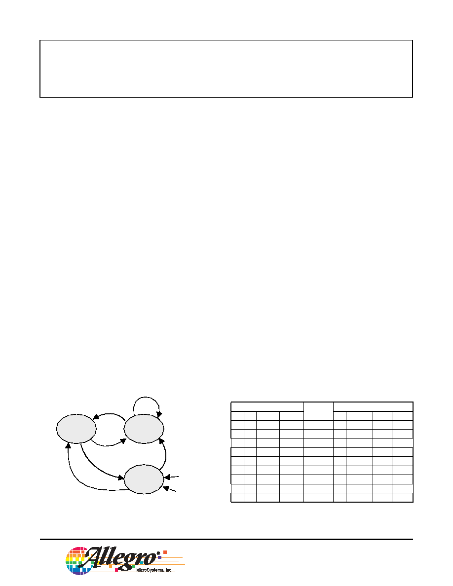
Operating Mode.
The A8423 has three modes of opera-
tion: Normal, Standby, and Sleep. The enable input, EN,
determines whether Normal mode is maintained (EN high)
Functional Description
Normal
Standby
Sleep
EN
1
Active=T
EN
0
EN
1
Active
T
POR
Active
F
UVLO
Active=F
EN
0
Figure 3. Operating state. Active is true (T) if WAKE is
low (L) or if LIN is low (L). Otherwise, Active is false (F).
The UVLO feature overrides.
Logic Functions
Inputs
State
Outputs
TX EN WAKE
LIN
RX
LIN
INH
VREG
1
1
*
H
Norm
Z
Rec(Z)
V
SUP
5V
1
1
*
L
Norm
L
Rec(Z)
V
SUP
5V
0
1
*
*
Norm
L
Dom(L)
V
SUP
5V
*
0
L
1
*
Standby
L
Rec(Z)
V
SUP
5V
*
0
*
L
1
Standby
L
Rec(Z)
V
SUP
5V
*
0
H
1
H
1
Sleep
Z
Rec(Z)
Z
Z
*
1
*
*
UVLO
Z
Rec(Z)
Z
Off
*
1
*
H
TSD
Z
Rec(Z)
V
SUP
5V
*
1
*
L
TSD
L
Rec(Z)
V
SUP
5V
1
Sleep mode is entered only when LIN is high, WAKE is high, and EN
goes to 0. The A8420/A8421 remains in Standby mode when WAKE
or LIN is low.
2
Z = High Impedance, * = Don't Care.

5
Worcester, Massachusetts 01615-0036 (508) 853-5000
115 Northeast Cutoff, Box 15036
www.allegromicro.com
Datasheet
A8423-DS Rev
.0
A8423
LIN Bus Transceiver with Integrated Voltage Regulator
Preliminary Subject to Change
Without Notice February 9, 2004
or one of the two inactive modes, Standby or Sleep, are
entered (EN low). If no other wake-up signals are active,
EN low sets the A8423 into low-current Sleep mode. From
Sleep mode the A8423 can be put directly into Normal
mode by taking EN high. Alternatively, it can be taken into
Standby mode by pulling the WAKE input to ground or by a
dominant state on the LIN Bus.
In Sleep mode, the supply current is at its minimum level,
and the LIN and RX pins are high impedance. In this mode,
the linear regulator is still active. When the power is fi rst
applied, the A8423 enters Sleep mode directly.
From Sleep mode, the A8423 may be taken through the
Standby mode, in which the RX output goes low to wake
up the protocol control device attached to the TX, RX, and
EN pins. Once the controller is active, it may then bring the
A8423 into Normal mode by taking EN high. If there is no
need to wake the controller prior to enabling the A8423, then
simply asserting EN high moves the A8423 directly from
Sleep mode to Normal mode.
The EN input has an internal pull-down resistor to ensure a
known safe state when the protocol controller is powered off.
The WAKE signal is a high-voltage input, which is designed
to allow a node on a sleeping bus to be awaken by a local
event. Sleep mode may be entered when WAKE is connected
directly to the battery or other similar voltage, such as VSUP.
To disable Sleep mode and allow the A8423 to enter Standby
mode, the WAKE input should be switched to ground.
The A8423 incorporates two protection functions. If the die
temperature becomes excessive, a thermal shutdown feature
(TSD) disables the LIN output dominant-state drive. Once
the temperature falls below the hysteresis level, the LIN out-
put resumes the state defi ned by the TX input. During TSD,
the output on VREG is maintained.
If the supply voltage drops below the UVLO threshold, all
outputs are disabled. When the supply voltage rises above
the UVLO threshold, the A8423 is reset into the Sleep mode.
From that state, it follows the logic shown in fi gure 1. That is,
if Active is true (T), the A8423 immediately goes to Standby
mode. If EN is high, it goes directly to the normal mode.
Linear Regulator
. The A8423 provides a linear regulator
output with specifi ed line and load regulation up to 30 mA
at 5 V. The regulator output is current-limited, at typically
100 mA. Care must be taken, however, when operating
above 30 mA, due to power dissipation. This is especially
important under fault conditions, such as load dump. This
output is active all modes, allowing a low-power microcon-
troller to continuously monitor sensor signals.
Power Dissipation.
Most power will normally be dissi-
pated in the linear regulator. Because the output of the regu-
lator is fi xed at 5 V, but the input supply can vary between
7 V and 18 V, care must be taken when setting the maximum
current. This is particularly important if the ability of the
A8423 to withstand a 40 V load dump is to be used.
The fi gures in the charts on the following page show the
allowable power dissipation and estimated maximum
current for various ambient temperatures and supply volt-
ages. The data were taken using a standard FR4 board with
minimal copper (R
JA
= 140ºC/W), and using a "High K"
dielectric board with copper ground plane and thermal vias
(R
JA
= 80ºC/W).