 | ÐлекÑÑоннÑй компоненÑ: A8430EEK | СкаÑаÑÑ:  PDF PDF  ZIP ZIP |
Äîêóìåíòàöèÿ è îïèñàíèÿ www.docs.chipfind.ru
Data Sheet
26185.300C
A8430
White LED Driver Constant Current Step-up Converter
Use the following complete part number when ordering:
AB SO LUTE MAX I MUM RAT INGS
SW Pin ................................................0.3 V to 36 V
Remaining Pins .................................. 0.3 V to 10 V
Ambient Operating Temperature, T
A
....... 40°C to 85°C
Junction Temperature, T
J(max)
...............................150°C
Storage Temperature, T
S
.................... 55°C to 150°C
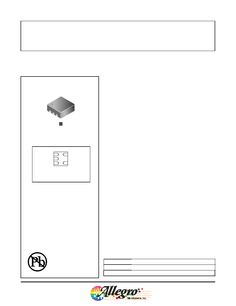
A8430 MLPD
Output voltage up to 36 V
2.5 V to 10 V input
Drives up to 4 LEDs at 20 mA from a 2.5 V supply
Drives up to 5 LEDs at 20 mA from a 3 V supply
1.2 MHz switching frequency
300 mA switch current limit
1 µA shutdown current
FEATURES
LED backlights
Portable battery-powered equipment
Cellular phones
PDAs (Personal Digital Assistant)
Camcorders, personal stereos, MP3 players, cameras
Mobile GPS systems
APPLICATIONS
The A8430 is a noninverting boost converter that steps-up the input
voltage, to provide a programmable constant current output at up to
36 V for driving white LEDs in series. Driving LEDs in series ensures
identical currents and uniform brightness. Up to four white LEDs can
be driven at 20 mA from a single cell Li-ion or a multicell NiMH power
source. Up to seven white LEDs can be driven by increasing the supply
voltage up to 10 V.
The A8430 incorporates a power switch and feedback sense amplifier
to provide a solution with minimum external components. The output
current can be set by adjusting a single external sense resistor and can
be varied with a voltage or filtered PWM signal when dimming control
is required. The high switching frequency of 1.2 MHz allows the use of
small inductor and capacitor values.
The A8430 is provided in a 5-pin 3 mm x 3 mm MLP package (part
number suffix EK), that has a nominal height of only 0.75 mm. The
lead-free version (part number suffix EK-T) has 100% lead-free matte
tin leadframe plating.
5
1
2
3
4
SW
GND
FB
VIN
EN
Part Number
Package
Description
A8430EEK
5-pin, MLPD
Surface Mount
A8430EEK-T
5-pin, MLPD
Lead-Free, Surface Mount
R
JA
= 50 °C/W, see note 1, page 2
Approximate actual size
Same pad footprint as SOT-23-5
2
Worcester, Massachusetts 01615-0036 (508) 853-5000
115 Northeast Cutoff, Box 15036
www.allegromicro.com
Data Sheet
26185.300C
A8430
White LED Driver Constant Current Step-up Converter
Characteristics
Symbol
Test Conditions
Min.
Typ.
Max.
Units
Input Voltage Range
V
IN
2.5
10
V
Supply Current
I
SUP
Active: I
LOAD
= 15 mA,
V
LOAD
= 12 V
2.5
3.5
mA
Shutdown (EN = 0 V)
0.1
1
µA
Feedback Reference Voltage
V
REF
86
95
104
mV
Feedback Input Current
I
FB
20
75
nA
Switch Current Limit
I
SWLIM
300
mA
Switch Frequency
F
SW
0.8
1.2
1.6
MHz
Switch Maximum Duty Cycle
D
85
90
%
Switch Saturation voltage
V
CE(SAT)
350
mV
Switch Leakage Current
I
SL
5
µA
Enable Input
Input Threshold Low
V
IL
0.4
V
Input Threshold High
V
IH
1.5
V
Input Leakage
Leakage
I
IL
1
µA
Note 1. Measured with 4-layer PCB. Please refer to application note "Package Thermal Characteristics," for thermal perfor-
mance measurement for 3 mm x 3 mm MLP package for additional information.
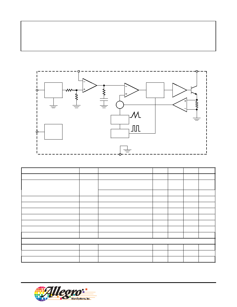
Functional Block Diagram
VIN
FB
SW
V
REF
1.25 V
GND
Driver
A2
S
Ramp
Generator
1.2 MHz
Oscillator
R
C
C
C
A1
95 mV
Enable
EN
R
Q
ELECTRICAL CHARACTERISTICS
at T
A
= 25°C, V
IN
= 3 V (unless otherwise noted)
3
Worcester, Massachusetts 01615-0036 (508) 853-5000
115 Northeast Cutoff, Box 15036
www.allegromicro.com
Data Sheet
26185.300C
A8430
White LED Driver Constant Current Step-up Converter
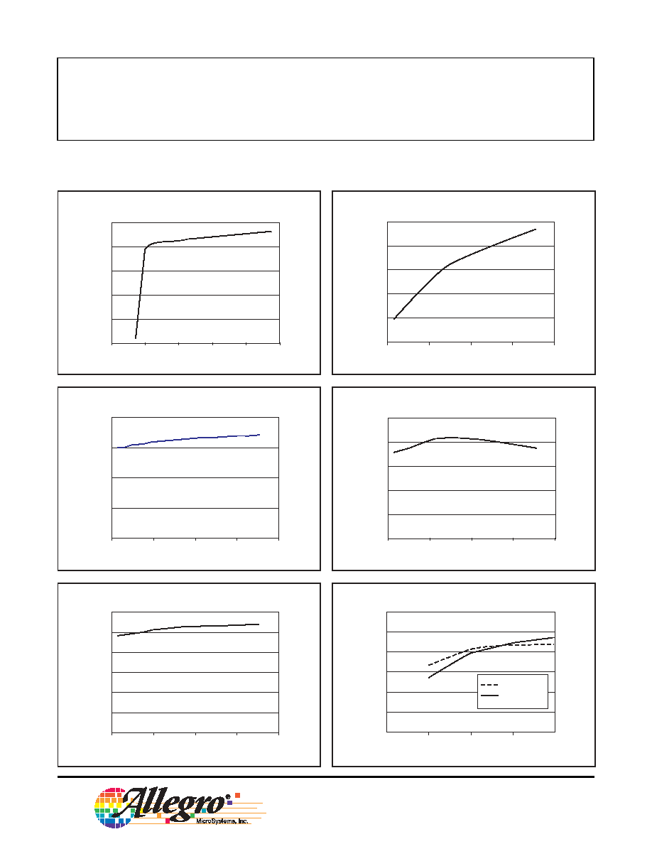
Operating Characteristics
Using Typical Application Circuit (Schematic 1)
60
65
70
75
80
85
90
0
5
10
15
20
LED Current (mA)
E
f
f
i
ci
en
cy
(
%
)
V
IN
= 3 V
V
IN
= 4 V
Quiescent Current versus Input Voltage
0
0.5
1.0
1.5
2.0
2.5
0
2
4
6
8
10
V
IN
(V)
Quiescent Current (mA)
Feedback Bias Current versus Temperature
0
5
10
15
20
Temperature (°C)
Feedback Bias Current (nA)
Switch Pin Voltage versus Temperature
Conversion Efficiency versus Current
0
100
50
150
200
250
300
Temperature (°C)
V
CE(SAT)
(mV)
Quiescent Current versus Temperature
1.90
1.95
2.00
2.05
2.10
2.15
50
0
50
100
150
Temperature (°C)
Quiescent Current (mA)
Switching Frequency versus Temperature
1.00
1.05
1.10
1.15
1.20
1.25
Temperature (°C)
Switching Frequency (MHz)
50
0
50
100
150
50
0
50
100
150
50
0
50
100
150
4
Worcester, Massachusetts 01615-0036 (508) 853-5000
115 Northeast Cutoff, Box 15036
www.allegromicro.com
Data Sheet
26185.300C
A8430
White LED Driver Constant Current Step-up Converter
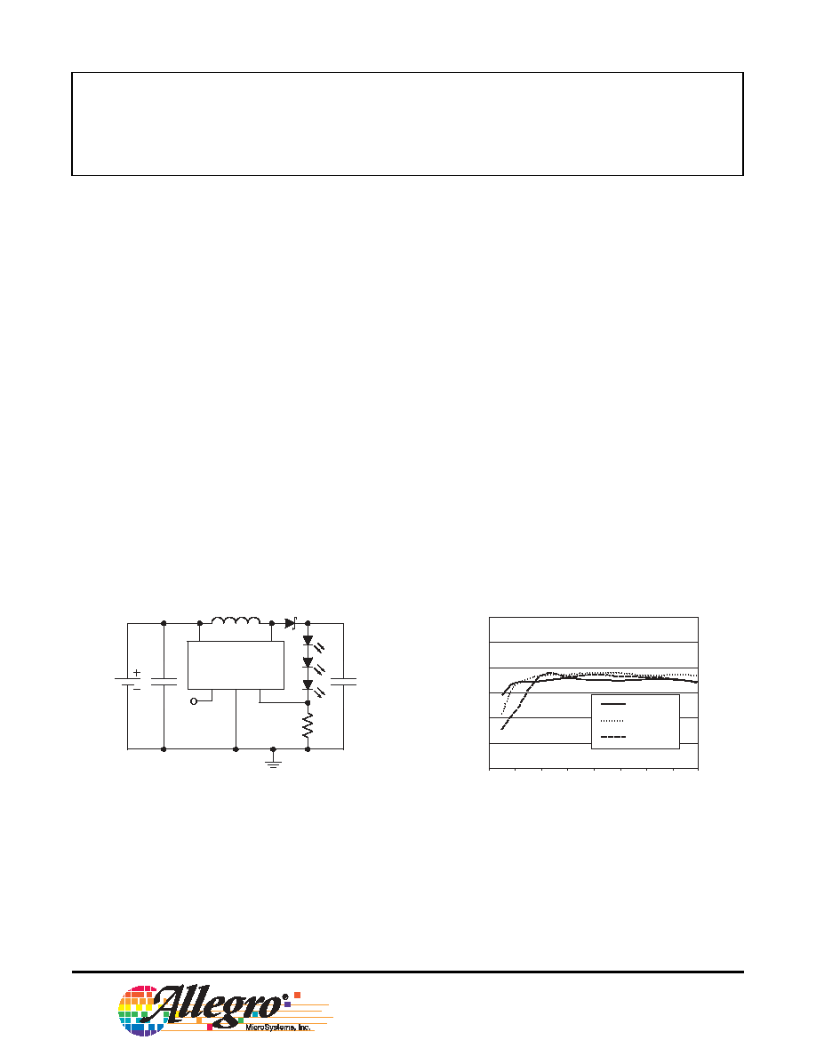
Functional Description
Schematic 1. Typical application
A8430
VIN
SW
EN
GND
FB
Li-ion
2.5V to
4.2V
C1
1µF
L1
22µH
D1
C2
0.22µF
R1
6.3
Enable
Typical Application
A typical application circuit for the A8430 is provided in
schematic diagram 1. This illustrates a method of driving
three white LEDs in series. The conversion efficiency of this
configuration is shown in chart 1.
Pin Functions
The diagram also shows a method of connecting the individ-
ual pins, whos functions are described as follows:
VIN. Supply to the control circuit. A bypass capacitor must be
connected from close to this pin to GND.
SW. Low-side switch connection between the inductor (L1)
and ground. Because rapid changes of current occur at this pin,
the traces on the PCB that are connected to this pin should be
minimized. In addition, the inductor (L1) and diode (D1) should
be connected as close to this pin as possible.
EN. Setting lower than 0.4 V disables the A8430 and puts the
control circuit into the low-power Sleep mode. Greater than
1.5 V fully enables the A8430.
GND. Ground reference connected directly to the ground plane.
The sense resistor (R1) should have a separate connection
directly to this point.
FB. Feedback pin for LED current control. The reference
voltage is 95 mV. The top of the sense resistor (R1) is typically
connected to this pin.
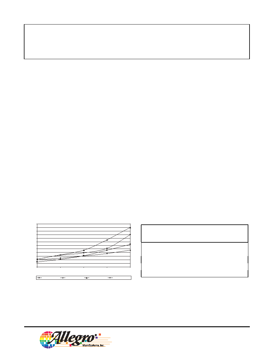
Conversion Efficiency versus Input Voltage
70
65
75
80
85
90
95
2
3
4
5
6
7
8
9
10
V
IN
(V)
Conversion Efficiency (%)
3 LEDs
4 LEDs
5 LEDs
Chart 1. Conversion efficiency when driving various
quantities of LEDs in the typical application circuit
5
Worcester, Massachusetts 01615-0036 (508) 853-5000
115 Northeast Cutoff, Box 15036
www.allegromicro.com
Data Sheet
26185.300C
A8430
White LED Driver Constant Current Step-up Converter
Device Operation
The A8430 uses a constant-frequency, current-mode control
scheme to regulate the current through the load. The load
current produces a voltage across the external sense resistor
(R1) and the input at the FB pin. This voltage is then
compared to the internal 95 mV reference to produce an error
signal. The switch current is sensed by the internal sense
resistor and compared to the load current error signal. As the
load current increases, the error signal diminishes, reducing
the maximum switch current and thus the current delivered
to the load. As
the load current
decreases, the error signal
rises, increasing the maximum switch current and thus
increasing the current delivered to the load.
To set
the load current,
ensure that the required internal
reference value of 95 mV is produced at the desired load. To
do so, select a resistance value for the sense resistor, R1 (),
such that:
R1 = 95 mV /
I
LOAD
where
I
LOAD
is the target load current (mA).
The table below shows typical values for R1. Note that the
resistance value is from the standard E96 series.
As load current is reduced, the energy required in the
inductor diminishes, resulting in the inductor current
dropping to zero for low load current levels. This is known
as Discontinuous mode operation, and results in some low-
frequency ripple. The average load current, however, remains
regulated down to zero.
In Discontinuous mode, when the inductor current drops to
zero, the voltage at the SW pin rings, due to the capacitance
in the resonant LC circuit formed by the inductor and the
capacitance of the switch and the diode. This ringing is
low-frequency and is not harmful. It can be damped with a
resistor across the inductor, but this reduces efficiency and is
not recommended.
Target Load Current
(
I
LOAD
)
(mA)
Sense Resistor (R1)
()
5
19.1
10
9.53
12
7.87
15
6.34
20
4.75
0
10
20
30
40
50
60
70
80
90
100
110
120
5
10
15
20
25
I
OUT
(mA)
PD (
m
W
)
Vin = 3V, 3 LED
Vin = 5V, 3 LED
Vin = 3V, 4 LED
Vin = 5V, 4 LED
Power Dissipation versus I
OUT