Äîêóìåíòàöèÿ è îïèñàíèÿ www.docs.chipfind.ru
A8483-DS, Rev. 1
1.2 MHz Step-up Converter
for Display Bias Supply
A8483
Output voltage up to 35 V
2.5 to 10 V input
0.9 to 18 V input with separate bias supply
Delivers 15 V at 15 mA with 2.7 V input
Constant 1.2 MHz switching frequency provides low noise
350 mA switch current limit
1 A shutdown current
Low-noise PWM/analog dimming
FEATURES
OLED bias supply / WLED backlight
Portable battery-powered equipment
Cellular phones
PDAs (Personal Digital Assistant)
Camcorders, personal stereos, MP3 players, cameras
Mobile GPS systems
APPLICATIONS
The A8483 is a current mode step-up dc-to-dc converter,
available in a 5-pin 3 mm × 3 mm thermally enhanced
MLP/TDFN lead (Pb) free package. Smaller external
components and integrated 36 V switch reduce component
count and footprint for a variety of applications.
A8483
VIN
V
SUPPLY
SW
EN
GND
FB
Li-ion
2.5 V to
5.5 V
C1
1 µF
L1
1
2
3
5
4
10 µH
D1
V
OUT
C2
1 µF
µ
R2
39 k
R1
820 k
Enable
OLED
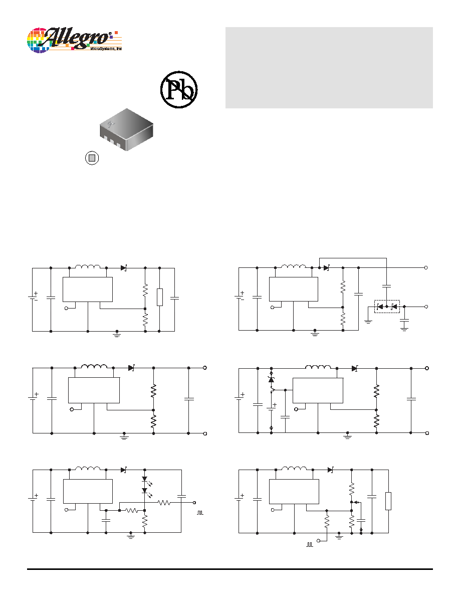
Figure 1.
OLED Bias Supply.
Use for cell phones, MP3
players, DSCs, and PDAs.
A8483
VIN
SW
EN
GND
FB
C1
1 µF
1
2
3
5
4
L1
10 µH
D1
D2
V
OUT1
+12 V
I
OUT1
+ I
OUT2
= 15 mA
V
OUT2
12 V
C2
0.47 µF
C3
0.47 µF
C4
0.47 µF
R2
39 k
R1
732 k
Enable
Li-ion
2.5 V to
5.5 V
V
SUPPLY
Figure 2.
Small LCD Bias Supply
. Li+ battery to ±12 V.
A8483
VIN
SW
EN
GND
FB
C1
1 µF
1
2
3
5
4
L1
10 µH
D1
V
OUT
C2
0.22 µF
Cf
0.01 µF
R2
5 k
Enable
R3
24 k
R1
47
Li-ion
2.5 V to
5.5 V
V
C
Analog Voltage or
PWM
V
SUPPLY
A8483
VIN
SW
EN
V
C
GND
FB
C1
1 µF
1
2
3
5
4
L1
10 µH
D1
V
OUT
C2
1 µF
R2
47 k
R1
560 k
Enable
R3
160 k
Cf
Cf for PWM dimming only
1 nF
OLED
Analog Voltage or
PWM 10 kHz
V
SUPPLY
Li-ion
2.5 V to
5.5 V
Figure 6.
OLED Bias Supply.
Use for low-noise PWM
dimming, or with analog voltage through the FB pin.
A8483
SW
EN
GND
VIN
5
FB
C1
1 µF
L1
1
2
3
4
10 µH
D1
5 V
V
OUT
C2
1 µF / 50 V
µ
R2
15 k
R1
768 k
for
V
OUT
= 32 V
604 k
for
V
OUT
= 25 V
Enable
32 V, 18 mA
25 V, 25 mA
V
SUPPLY
Figure 3.
LCD TV, Plasma TV Bias, FED Display,
Varactor Diode Bias.
Using 5 V input.
A8483
VIN
SW
EN
GND
FB
7.5 V
V
Z
C1
1 µF
C3
0.1 µF
L1
1
2
3
5
4
22 µH
D1
12 V
V
OUT
C2
1 µF / 50 V
µ
R2
15 k
R1
768 k
for
V
OUT
= 32 V
604 k
for
V
OUT
= 25 V
Enable
32 V, 40 mA
25 V, 80 mA
Connect either V
Z
or V
BIAS
V
SUPPLY
5 V
V
BIAS
Figure 4.
LCD TV, Plasma TV Bias, FED Display,
Varactor Diode Bias.
Using 12 V input.
Figure 5.
WLED Backlighting
.
Approximate Scale 1:1
Package EK:
MLP/TDFN, 3 × 3 mm
0.75 mm Nominal Height
A8483-DS, Rev. 1
Worcester, Massachusetts 01615-0036 (508) 853-5000
115 Northeast Cutoff, Box 15036
www.allegromicro.com
Allegro MicroSystems, Inc.
1.2 MHz Step-up Converter for Display Bias Supply
A8483
2
Functional Block Diagram
VIN
FB
SW
V
REF
1.25 V
GND
Driver
A2
S
Ramp
Generator
1.2 MHz
Oscillator
R
C
C
C
A1
615 mV
Enable
EN
R
Q
Terminal List Table
Pin
Name
Function
1
SW
Internal power FET
2
GND
Ground
3
FB
Feedback input
4
EN
Enable input
5
VIN
Input supply
Ab so lute Max i mum Rat ings
SW Pin ..................................................................................0.3 to 36 V
Remaining Pins .................................................................... 0.3 to 10 V
Operating Ambient Temperature
, T
A
.................................... 40°C to 85°C
Junction Temperature, T
J(max)
............................................................. 150°C
Storage Temperature, T
S
.................................................. 55°C to 150°C
5
1
2
3
4
SW
GND
FB
VIN
EN
Device Pin-out Diagram
R
JA
= 50 °C/W, on a 4-layer board. Additional information is
available on the Allegro Web site.
Package Thermal Characteristics

A8483-DS, Rev. 1
Worcester, Massachusetts 01615-0036 (508) 853-5000
115 Northeast Cutoff, Box 15036
www.allegromicro.com
Allegro MicroSystems, Inc.
1.2 MHz Step-up Converter for Display Bias Supply
A8483
3
Characteristics
Symbol
Test Conditions
Min.
Typ.
Max.
Units
Input Voltage Range
V
IN
2.5
10
V
Supply Current
I
SUP
Active: I
OUT
= 15 mA, V
OUT
= 12 V
2.5
3.5
mA
Shutdown (EN = 0 V)
0.1
1
A
Feedback Reference Voltage
V
FB
590
615
640
mV
Feedback Input Current
I
FB
V
FB
= 0.615 V
50
100
nA
Switch Current Limit
I
SWLIM
350
mA
Switch Frequency
F
SW
0.8
1.2
1.6
MHz
Switch Maximum Duty Cycle
D
85
90
%
Switch Saturation voltage
V
CE(SAT)
I
SW
= 0.2 A
350
mV
Switch Leakage Current
I
SL
V
SW
= 36 V
5
A
Enable Input
Input Threshold Low
V
IL
0.4
V
Input Threshold High
V
IH
1.5
V
Input Leakage
Leakage
I
IL
1
A
ELECTRICAL CHARACTERISTICS
at T
A
= 25°C, V
IN
= 3 V (unless otherwise noted)
Operating Characteristics
(V
IN
= 3 V)
Efficiency versus Input Voltage
V
OUT
= 15 V; Toko 1098AS-100M Inductor
V
FB
= 0.615 V
50
2
3
4
6
5
8
9
7
10
V
IN
(V)
Efficiency (%)
Switching Frequency versus Temperature
1.00
1.05
1.10
1.15
1.20
1.25
Temperature (°C)
F
SW
(MHz)
Feedback Bias Current versus Temperature
50
53
56
59
62
65
50
0
50
100
150
Temperature (°C)
I FB
(nA)
Quiescent Supply Current versus Temperature
2.1
2.2
2.3
2.4
2.5
2.6
Temperature (°C)
I
SUPQ
(mA)
50
0
50
100
150
50
0
50
100
150
55
60
70
80
75
90
85
65
I
OUT (mA)
25
15
2
A8483-DS, Rev. 1
Worcester, Massachusetts 01615-0036 (508) 853-5000
115 Northeast Cutoff, Box 15036
www.allegromicro.com
Allegro MicroSystems, Inc.
1.2 MHz Step-up Converter for Display Bias Supply
A8483
4
Functional Description
Pin Functions
VIN. Supply to the control circuit. A bypass capacitor, C1, must
be connected from close to this pin to GND.
GND. Ground reference connected directly to the ground plane.
The feedback resistor should have a separate connection directly
to this point.
EN. Voltage lower than 0.4 V disables the A8483 and puts the
control circuit into the low-power sleep mode. Voltage greater
than 1.5 V fully enables the A8483.
SW. Low-side switch connection between the inductor, L1,
and ground. Because rapid changes of current occur at this
pin, the traces on the PCB that are connected to this pin should
be minimized. In addition, L1 and the diode, D1, should be
connected as close to this pin as possible.
FB. Feedback pin for OLED voltage control or WLED current
control. The reference voltage is 615 mV. Connect the feedback
resistor close to this pin to minimize noise.
Device Operation
The A8483 uses a 1.2 MHz constant switching frequency current-
mode control scheme to regulate the output voltage or current
through the load.
A typical OLED bias supply is shown in figure 7. For driving
OLEDs, output voltage is sensed by the FB pin through a voltage
divider network. Output voltage, V
OUT
(V), is set according to the
following equation:
2
2
1
=
+
V
OUT
R
R
R
0.615 .
(1)
A typical WLED backlight supply is shown in figure 8. The load
current, I
LOAD
, is set by the selecting the external sense resistor,
R1, to produce 615 mV at the desired load, for example:
=
1
R
0.615 I
LOAD
.
(2)
Voltage sensed across the FB pin is compared with the internal
615 mV reference to produce an error signal. The switch current
is sensed by the internal sense resistor and compared to the
error signal for current mode PWM control. As the error signal
increases, I
LOAD
, increases to increase either output voltage,
V
OUT
, or current, I
OUT
, such that the FB pin voltage follows the
internal 615 mV reference voltage.
As I
LOAD
is reduced, the energy required in the inductor, L1, also
reduces, resulting in the inductor current dropping to zero for
low load current levels. This is known as Discontinuous mode
operation and results in some low-frequency ripple. The average
load current will, however, remain regulated down to zero. In
Discontinuous mode, when I
LOAD
drops to zero, the voltage at
the SW pin rings, due to the resonant LC circuit formed by L1
and the switch and diode D1 capacitance. This ringing is low-
frequency and is not harmful. It can be damped with a resistor
across the inductor but this will reduce efficiency and is not
recommended.
A8483
VIN
V
SUPPLY
SW
EN
GND
FB
Li-ion
2.5 V to
5.5 V
C1
1 µF
L1
1
2
3
5
4
10 µH
D1
V
OUT
C2
1 µF
µ
R2
39 k
R1
820 k
Enable
OLED
Figure 7. OLED Bias Supply. Use for cell phones, MP3 players, DSCs,
and PDAs. (Circuit also shown in figure 1.)
A8483
VIN
SW
EN
GND
FB
C1
1 µF
1
2
3
5
4
L1
10 µH
D1
V
OUT
C2
0.22 µF
Cf
0.01 µF
R2
5 k
Enable
R3
24 k
R1
47
Li-ion
2.5 V to
5.5 V
V
C
Analog Voltage or
PWM
V
SUPPLY
Figure 8. WLED Backlighting. (Circuit also shown in figure 5.)
A8483-DS, Rev. 1
Worcester, Massachusetts 01615-0036 (508) 853-5000
115 Northeast Cutoff, Box 15036
www.allegromicro.com
Allegro MicroSystems, Inc.
1.2 MHz Step-up Converter for Display Bias Supply
A8483
5
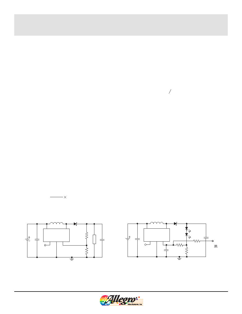
Dimming Control
Display dimming can be achieved by controlling the output
voltage, V
OUT
, using the FB pin. The circuitry behind the FB
pin is flexible, to accommodate a variety of schemes used for
dimming:
· Adjust the duty cycle of the pulse train applied to the FB pin
through resistor R3, as shown in figure 11. Capacitor Cf is
used to generate the average voltage level. Variation of output
voltage with PWM duty cycle is shown in figure 9.
· Apply a constant dc voltage to the FB pin through resistor
R3, as shown in figure 12. Variation of output voltage with dc
voltage are shown in figure 10.
· Selection of the resistor connected between the FB pin and
GND, as shown in figure 12 for OLED applications, and in
figure 13 for WLED applications. The voltage drop across
the transistor should be negligible compared to the FB sense
voltage.
Soft Start
Output voltage rise time at power-on can be extended by using a
soft start circuit, such as the one shown in figure 14 for an OLED
application, and in figure 16 for a WLED application. At power-
on, the device duty cycle begins initially at a high level, drawing
a large current from the input supply, VIN. The soft-start circuits
shown can reduce the level of current flow by controlling the FB
pin.
When a signal is applied to the EN pin, capacitor C3 discharges,
pulling the FB pin high, and reducing V
OUT
to a minimum.
When the EN signal is removed, C3 recharges and as it does, the
voltage drop across R3 reduces, allowing the device duty cycle to
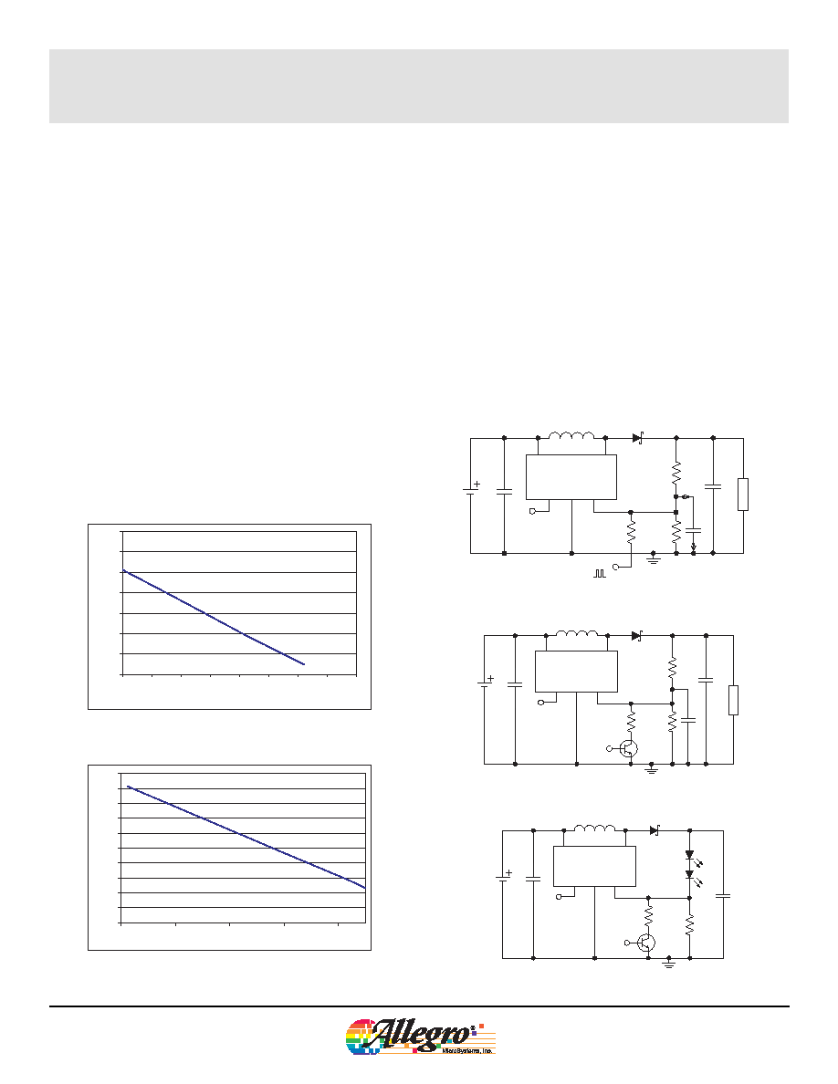
Figure 9. PWM Dimming Control of Duty Cycle. Performance of 5 V input
circuit shown in figure 3.
3
5
7
9
11
13
15
17
10
20
30
40
50
60
70
80
90
Duty Cycle (%)
V
OUT
(V
)
0
2
4
6
8
10
12
14
16
18
20
0.2
0.4
0.6
0.8
1
V
C
(V)
V
OUT
(V
)
Figure 10. DC Voltage Dimming Control of Duty Cycle. Performance of
circuit shown in figure 11.
Figure 12. OLED Dimming Control. Single-bit resolution using
external transistor.
A8483
VIN
SW
EN
V
C
GND
FB
C1
1 µF
1
2
3
5
4
L1
10 µH
Q1
D1
V
OUT
C2
10 µF
R2
47 k
R1
560 k
Enable
R3
47 k
Cf
1 nF
OLED
V
SUPPLY
Li-ion
2.5 V to
5.5 V
Figure 13. WLED Dimming Control. Single-bit resolution using
external transistor.
A8483
VIN
SW
EN
V
C
GND
FB
C1
1 µF
1
2
3
5
4
L1
10 µH
Q1
D1
V
OUT
C2
0.22 µF
Enable
R2
80
R1
80
V
SUPPLY
Li-ion
2.5 V to
5.5 V
Applications Information
A8483
VIN
SW
EN
V
C
GND
FB
C1
1 µF
1
2
3
5
4
L1
10 µH
D1
V
OUT
C2
1 µF
R2
47 k
R1
560 k
Enable
R3
160 k
Cf
Cf for PWM dimming only
1 nF
OLED
Analog Voltage or
PWM 10 kHz
V
SUPPLY
Li-ion
2.5 V to
5.5 V
Figure 11. OLED Bias Supply. Use for low-noise PWM dimming,
or with analog voltage through the FB pin.