 | –≠–ª–µ–∫—Ç—Ä–æ–Ω–Ω—ã–π –∫–æ–º–ø–æ–Ω–µ–Ω—Ç: A8499 | –°–∫–∞—á–∞—Ç—å:  PDF PDF  ZIP ZIP |
A8499-DS
High Voltage Step-Down
Regulator
A8499
8 to 50 V input range
Integrated DMOS switch
Adjustable fixed off-time
Highly efficient
Adjustable 1.2 to 24 V output
Package LJ, 8-pin SOIC
with exposed thermal pad
FEATURES
Printer power supplies
Consumer equipment power supplies
APPLICATIONS
The A8499 is a step down regulator that will handle a
wide input operating voltage range.
The A8499 is supplied in a low-profile 8-lead SOIC
with exposed pad (package LJ).
VIN
LX
BOOT
ENB
TSET
GND
VBIAS
FB
+42 V
220 F
10 V
ESR
VOUT
COUT
3.3 V / 1.2 A
17.8 k
R1
L 1
D1
R2
10.2 k
0.22 F
0.01 F
CBOOT
C3
C3
RTSET
121 k
47 H
100 F
50 V
A8499
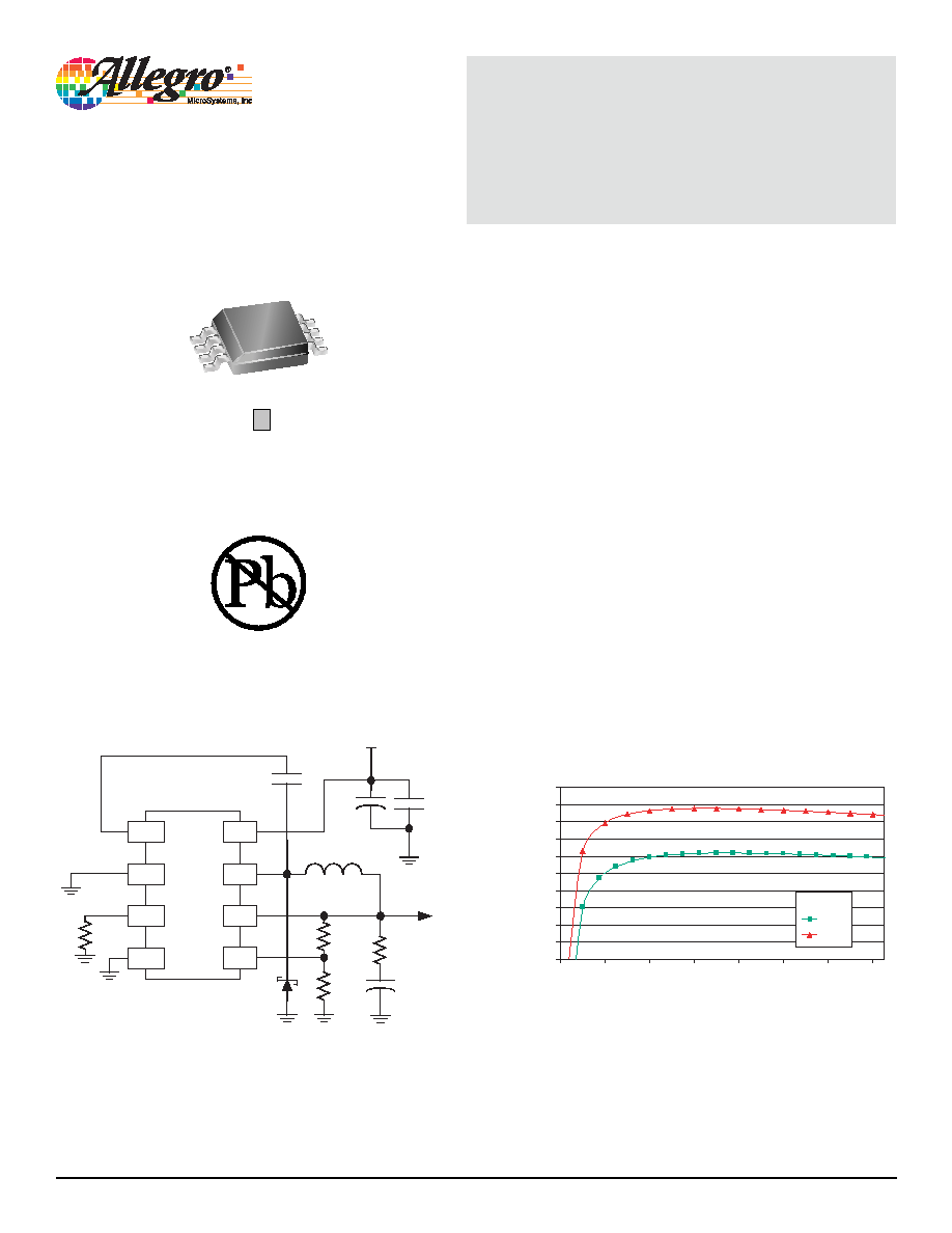
Efficiency vs. Output Current
70.0
72.0
74.0
76.0
78.0
80.0
82.0
84.0
86.0
88.0
90.0
0
200
400
600
800
1000
1200
1400
I
OUT
(mA)
E
f
f
i
ci
e
n
cy
%
3.3
5
V
OUT
(V)
Circuit for 42 V step down to 3.3 V at 1.2 A. Efficiency data from circuit shown in left panel.Data is for reference only.
TYPICAL APPLICATION
Approximate Scale 1:1

A8499-DS
Allegro MicroSystems, Inc.
115 Northeast Cutoff, Box 15036
Worcester, Massachusetts 01615-0036 (508) 853-5000
www.allegromicro.com
A8499
High Voltage Step-Down Regulator
2
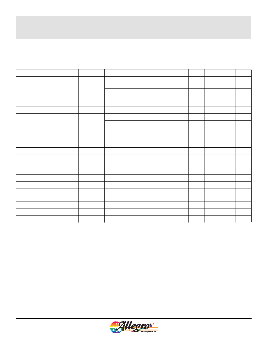
Functional Block Diagram
Ab so lute Max i mum Rat ings
Package Thermal Characteristics*
Package
R
JA
(∞C/W)
PCB
LJ
35
4-layer
* Additional information is available on the Allegro Web site
Supply Voltage, V
IN
.........................................................................50 V
VBIAS Input Voltage, V
BIAS
.................................................≠0.3 to 7 V
Switch Voltage, V
LX
........................................................................≠1 V
ENB Input Voltage, V
ENB
......................................................≠0.3 to 7 V
Junction Temperature, T
J(max)
....................................................... 150∞C
Storage Temperature, T
S
............................................... ≠55∞C to 150∞C
Operating Ambient Temperature, T
A
............................... ≠20∞C to 85∞C
+
≠
+
≠
+
≠
BOOT
ENB
TSET
GND
VIN
LX
FB
VBIAS
Switch PWM
C
Soft Start
Ramp Generation
COMP
1.2 V
Boot Charge
VBIAS is connected to VOUT
when V
OUT
target is between
3.3 and 5 V
D1
L1
V
IN
COUT
VOUT
ESR
UVLO
TSD
Switch
Disable
Bias Supply
I_Peak
I_Demand
Clamp
Use the following complete part number when ordering:
Part Number
Packing
Description
A8499SLJTR-T
13-in. reel,
3000 pieces/reel
Surface
Mount
Leadframe plating 100% matte-tin.
A8499-DS
Allegro MicroSystems, Inc.
115 Northeast Cutoff, Box 15036
Worcester, Massachusetts 01615-0036 (508) 853-5000
www.allegromicro.com
A8499
High Voltage Step-Down Regulator
3
Characteristics
Symbol
Test Conditions
Min.
Typ.
Max.
Units
VIN Quiescent Current
I
VIN(Q)
V
ENB
= LOW, I
OUT
= 0 mA, V
IN
= 42 V
V
BIAS
= V
OUT
(see note
3
)
≠
0.90
1.35
mA
V
ENB
= LOW, I
OUT
= 0 mA, V
IN
= 42 V
V
BIAS
< 3 V
≠
4.4
6.35
mA
V
ENB
= HIGH
≠
≠
100
A
VBIAS Input Current
I
BIAS
V
BIAS
= V
OUT
≠
3.5
5
mA
Buck Switch On Resistance
R
DS(on)
T
A
= 25∞C, I
OUT
= 2 A
≠
700
800
m
T
A
= 125∞C, I
OUT
= 2 A
≠
≠
1.6
Fixed Off-Time Proportion
Based on calculated value
≠15
≠
15
%
Feedback Voltage
V
FB
1.176
1.200
1.224
V
Output Voltage Regulation
I
OUT
= 0 mA to 2 A
≠3
≠
3
%
Feedback Input Bias Current
I
FB
≠400
≠100
100
nA
Soft Start Time
t
ss
5
10
15
ms
Buck Switch Current Limit
I
CL
V
FB
> 0.5 V
2.2
≠
3
A
V
FB
< 0.5 V
0.5
≠
1.2
A
ENB Open Circuit Voltage
V
OC
Output disabled
2.0
≠
7
V
ENB Input Voltage Threshold
V
ENB(0)
LOW level input (Logic 0), output enabled
≠
≠
1.0
V
ENB Input Current
I
ENB(0)
V
ENB
= 0 V
≠10
≠
≠1
A
VIN Undervoltage Threshold
V
UVLO
V
IN
rising
≠
6.9
7.1
V
VIN Undervoltage Hysteresis
V
UVLOHYS
V
IN
falling
0.7
≠
1.1
V
Thermal Shutdown Temperature
T
JTSD
Temperature increasing
≠
165
≠
∞C
Thermal Shutdown Hysteresis
T
J
Recovery = T
JTSD
≠ T
J
≠
15
≠
∞C
1. Negative current is defined as coming out of (sourcing) the specified device pin.
2. Specifications over the junction temperature range of 0∫C to 125∫C are assured by design and characterization.
3. VBIAS is connected to VOUT node when V
OUT
target level is between 3.3 and 5 V.
ELECTRICAL CHARACTERISTICS
1,2
at T
A
= 25∞C, V
IN
= 8 to 50 V (unless noted otherwise)
A8499-DS
Allegro MicroSystems, Inc.
115 Northeast Cutoff, Box 15036
Worcester, Massachusetts 01615-0036 (508) 853-5000
www.allegromicro.com
A8499
High Voltage Step-Down Regulator
4
Functional Description
The A8499 is a fixed off-time, current-mode≠controlled buck
switching regulator. The regulator requires an external clamping
diode, inductor, and filter capacitor, and operates in both continu-
ous and discontinuous modes. An internal blanking circuit is used
to filter out transients resulting from the reverse recovery of the
external clamp diode. Typical blanking time is 200 ns.
The value of a resistor between the TSET pin and ground deter-
mines the fixed off-time (see graph in the t
off
section).
V
OUT
. The output voltage is adjustable from 1.2 to 24 V, based on
the combination of the value of the external resistor divider and
the internal 1.2 V ±3% reference. The voltage can be calculated
with the following formula:
V
OUT
= V
FB
◊ (1 + R1/R2)
(1)
Light Load Regulation. To maintain voltage regulation during
light load conditions, the switching regulator enters a cycle-skip-
ping mode. As the output current decreases, there remains some
energy that is stored during the power switch minimum on-time.
In order to prevent the output voltage from rising, the regulator
skips cycles once it reaches the minimum on-time, effectively
making the off-time larger.
Soft Start. An internal ramp generator and counter allow the out-
put to slowly ramp up. This limits the maximum demand on the
external power supply by controlling the inrush current required
to charge the external capacitor and any dc load at startup.
Internally, the ramp is set to 10 ms nominal rise time. During soft
start, current limit is 2.2 A minimum.
The following conditions are required to trigger a soft start:
∑ V
IN
> 6 V
∑ ENB pin input falling edge
∑ Reset of a TSD (thermal shut down) event
V
BIAS
. To improve overall system efficiency, the regulator output,
V
OUT
, is connected to the VBIAS input to supply the operating
bias current during normal operating conditions. During start up
the circuitry is run off of the VIN supply. VBIAS should be con-
nected to VOUT when the V
OUT
target level is between 3.3 and
5 V. If the output voltage is less than 3.3 V, then the A8499 can
operate with an internal supply and pay a penalty in efficiency,
as the bias current will come from the high voltage supply, VIN.
VBIAS can also be supplied with an external voltage source. No
power-up sequencing is required for normal opperation.
ON/OFF Control. The ENB pin is externally pulled to ground
to enable the device and begin the soft start sequence. When the
ENB is open circuited, the switcher is disabled and the output
decays to 0 V.
Protection. The buck switch will be disabled under one or more
of the following fault conditions:
∑ V
IN
< 6 V
∑ ENB pin = open circuit
∑ TSD fault
When the device comes out of a TSD fault, it will go into a soft
start to limit inrush current.
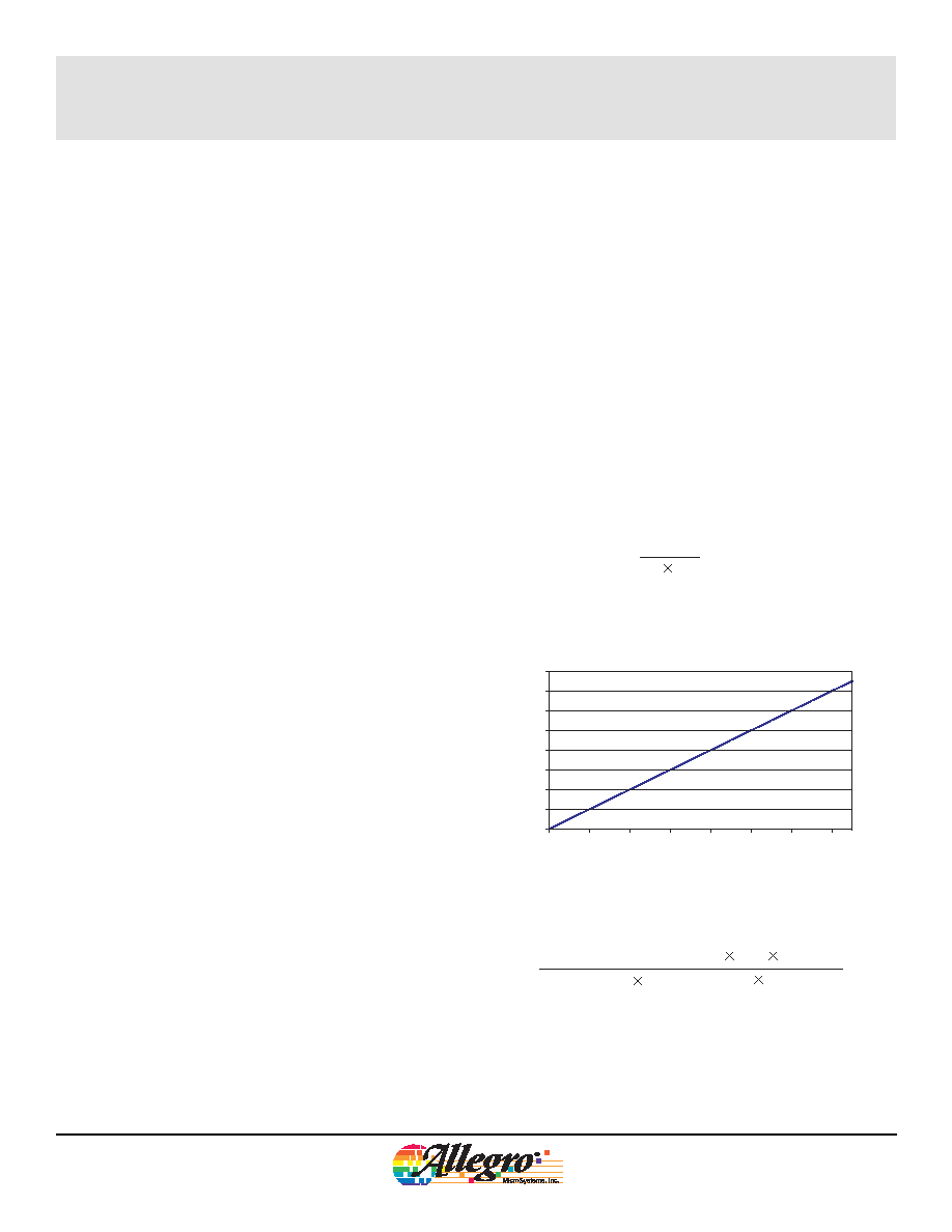
t
OFF
. The value of a resistor between the TSET pin and ground
determines the fixed off-time. The formula to calculate t
OFF
(s)
is:
TSET
=
t
OFF
1.2 10
10
R
,
(2)
where R
TSET
(k) is the value of the resistor. Results are shown
in the following graph:
t
ON
. From the volt-second balance of the inductor, the turn-on
time, t
ON
, can be calculated approximately by the equation:
=
t
ON
(V
OUT
+
V
f
+
I
OUT
R
L
) t
OFF
V
IN
≠
I
OUT
R
DS(on)
≠
I
OUT
R
L
≠
V
OUT
(3)
where
V
f
is the voltage drop across the external Schottky diode,
R
L
is the winding resistance of the inductor, and
R
DS(on)
is the on-resistance of the switching MOSFET.
Resistance vs. Off-Time
1
3
5
7
9
11
13
15
17
12
36
60
84
108
132
156
180
R
TSET
(k)
t
OFF
(
s
)

A8499-DS
Allegro MicroSystems, Inc.
115 Northeast Cutoff, Box 15036
Worcester, Massachusetts 01615-0036 (508) 853-5000
www.allegromicro.com
A8499
High Voltage Step-Down Regulator
5
The switching frequency is calculated as follows:
=
f
SW
1
t
ON
+
t
OFF
(4)
Shorted Load. If the voltage on the FB pin falls below 0.5 V, the
regulator will invoke a 0.8 A typical overcurrent limit to handle
shorted load condition at the regulator output. For low output
voltages at power up and in the case of a shorted output, the off-
time is extended to prevent loss of control of the current limit due
to the minimum on-time of the switcher.
The extension of the off-time is based on the value of the TSET
multiplier and the FB voltage, as shown in the following table:
V
FB
(V)
TSET Multiplier
< 0.25
8 ◊ t
OFF
< 0.50
4 ◊ t
OFF
< 0.75
2 ◊ t
OFF
> 0.75
t
OFF
Component Selection
L1. The inductor must be rated to handle the total load current.
The value should be chosen to keep the ripple current to a reason-
able value. The ripple current, I
RIPPLE
, can be calculated by:
I
RIPPLE
= V
L(OFF)
◊ t
OFF
/ L
(5)
V
L(OFF)
= V
OUT
+ V
f
+ I
L(AVG)
◊ R
L
(6)
Example:
Given V
OUT
= 5 V, V
f
= 0.55 V, V
IN
= 42 V, I
LOAD
= 0.5 A, power
inductor with L = 180 H and R
L
= 0.5 Rdc at 55∞C, t
OFF
=
7 s, and R
DS(on)
= 1 .
Substituting into equation 6:
V
L(OFF)
= 5 V + 0.55 V+ 0.5 A ◊ 0.5 = 5.8 V
Substituting into equation 5:
I
RIPPLE
= 5.8 V ◊ 7 s / 180 H = 225 mA
The switching frequency, f
SW
, can then be estimated by:
f
SW
= 1 / ( t
ON
+ t
OFF
)
(7)
t
ON
= I
RIPPLE
◊ L / V
L(ON)
(8)
V
L(ON)
= V
IN
≠ I
L(AVG)
◊ R
DS(on)
≠
I
L(AVG)
◊ R
L
≠ V
OUT
(9)
Substituting into equation 9:
V
L(ON)
= 42 V ≠ 0.5 A ◊ 1 ≠ 0.5 A ◊ 0.5 ≠ 5 V = 36 V
Substituting into equation 8:
t
ON
= 225 mA ◊ 180 H / 36 V = 1.12 s
Substituting into equation 7:
f
SW
= 1 / (7 s +1.12 s) = 123 kHz
Higher inductor values can be chosen to lower the ripple cur-
rent. This may be an option if it is required to increase the total
maximum current available above that drawn from the switching
regulator. The maximum total current available, I
LOAD(MAX)
, is:
I
LOAD(MAX)
= I
CL(MIN)
◊ t
OFF
/ L
(5)
where I
CL(MIN)
is 2.2 A, from the Electrical Chracteristics table.
D1. The Schottky catch diode should be rated to handle 1.2 times
the maximum load current. The voltage rating should be higher
than the maximum input voltage expected during all operating
conditions. The duty cycle for high input voltages can be very
close to 100%.
COUT. The main consideration in selecting an output capacitor
is voltage ripple on the output. For electrolytic output capacitors,
a low-ESR type is recommended.
The peak-to-peak output voltage ripple is simply I
RIPPLE
◊ ESR.
Note that increasing the inductor value can decrease the ripple
current. The minimum voltage rating of the capacitor is 10 V,
however, because ESR decreases with voltage, the most cost-
effective choice may be rated higher in voltage. The ESR should
be in the range from 50 to 500 m.