 | –≠–ª–µ–∫—Ç—Ä–æ–Ω–Ω—ã–π –∫–æ–º–ø–æ–Ω–µ–Ω—Ç: A8902 | –°–∫–∞—á–∞—Ç—å:  PDF PDF  ZIP ZIP |
Dwg. PP-040B
ABSOLUTE MAXIMUM RATINGS
at T
A
= +25
∞
C
Load Supply Voltage, V
BB
. . . . . . . . . . 14 V
Output Current, I
OUT
. . . . . . . . . . . .
±
1.25 A
Logic Supply Voltage, V
DD
. . . . . . . . . 6.0 V
Logic Input Voltage Range,
V
IN
. . . . . . . . . . . -0.3 V to V
DD
+ 0.3 V
Package Power Dissipation, P
D
See Graph
Operating Temperature Range,
T
A
. . . . . . . . . . . . . . . . . . 0
∞
C to +70
∞
C
Junction Temperature, T
J
. . . . . . . +150
∞
C
Storage Temperature Range,
T
S
. . . . . . . . . . . . . . . -55
∞
C to +150
∞
C
Fault conditions that produce excessive junction
temperature will activate device thermal shutdown
circuitry. These conditions can be tolerated, but
should be avoided.
Output current rating may be restricted to a value
determined by system concerns and factors.
These include: system duty cycle and timing,
ambient temperature, and use of any heatsinking
and/or forced cooling. For reliable operation, the
specified maximum junction temperature should
not be exceeded.
Always order by complete part number, e.g., A8902CLBA .
Data Sheet
26301.2
The A8902CLBA is a three-phase brushless dc motor controller/
driver for use in 5 V or 12 V hard-disk drives. The three half-bridge
outputs are low on-resistance n-channel DMOS devices capable of
driving up to 1.25 A. The A8902CLBA provides complete, reliable,
self-contained back-EMF sensing motor startup and running algorithms.
A programmable digital frequency-locked loop speed control circuit
together with the linear current control circuitry provides precise motor
speed regulation.
A serial port allows the user to program various features and
modes of operation, such as the speed control parameters, startup
current limit, sleep mode, diagnostic modes, and others.
The A8902CLBA is fabricated in Allegro's BCD (Bipolar CMOS
DMOS) process, an advanced mixed-signal technology that combines
bipolar, analog and digital CMOS, and DMOS power devices. The
A8902CLBA is provided in a 24-lead wide-body SOIC batwing package.
It provides for the smallest possible construction in surface-mount
applications.
FEATURES
s
DMOS Outputs
s
Low r
DS(on)
s
Startup Commutation Circuitry
s
Back-EMF Commutation Circuitry
s
Serial Port Interface
s
Frequency-Locked Loop Speed Control
s
Sector Data Tachometer Signal Input
s
Programmable Start-Up Current
s
Diagnostics Mode
s
Sleep Mode
s
Linear Current Control
s
Internal Current Sensing
s
Dynamic Braking Through Serial Port
s
Power-Down Dynamic Braking
s
System Diagnostics Data Out
s
Data Out Ported in Real Time
s
Internal Thermal Shutdown Circuitry
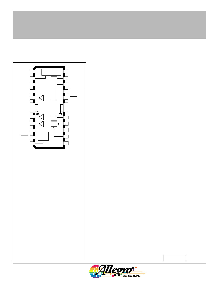
3-PHASE BRUSHLESS DC MOTOR
CONTROLLER/DRIVER WITH BACK-EMF SENSING
1
2
3
4
5
6
7
8
9
24
23
22
21
20
19
18
17
16
15
14
13
12
11
10
9
BRAKE
FILTER
DATA IN
LOGIC
SUPPLY
GROUND
CHIP SELECT
CLOCK
RESET
GROUND
GROUND
GROUND
DD
V
C
ST
OUTA
OUTB
OUTC
C D1
BB
V
LOAD
SUPPLY
C WD
C D2
DATA OUT
SECTOR
DATA
CENTERTAP
OSCILLATOR
C RES
SERIAL PORT
FLL
MUX
COMMUTATION
DELAY
BOOST
CHARGE
PUMP
8902≠A

8902≠A
3-PHASE BRUSHLESS DC
MOTOR CONTROLLER/DRIVER
115 Northeast Cutoff, Box 15036
Worcester, Massachusetts 01615-0036 (508) 853-5000
FUNCTIONAL BLOCK DIAGRAM
CURRENT
CONTROL
Dwg. FP-034
22
21
23
17
20
CENTERTAP
10
C WD
3
OSC
16
SECTOR
DATA
14
FILTER
13
C ST
4
C RES
12
BRAKE
11
OUT A
OUT B
OUTC
COMMUTATION
LOGIC
COMMUTATION
DELAY
C D1
C D2
24
2
WATCHDOG
TIMER
SEQUENCE
LOGIC
BLANK
FCOM
OUT A
5
OUT B
8
OUTC
9
1
LOAD
SUPPLY
V
BB
CHARGE
PUMP
FREQUENCY-
LOCKED LOOP
SERIAL PORT
MUX
CLOCK
DATA IN
DATA
OUT
CHIP
SELECT
RESET
TSD
R
S
15
V
DD
LOGIC
SUPPLY
START-UP
OSC.
BOOST
CHARGE
PUMP
BRAKE
18-19
6-7
GROUND
GROUND
50
75
100
125
150
2.5
1.5
1.0
0.5
0
TEMPERATURE in
∞
C
2.0
25
Dwg. GP-019B
R = 6
∞
C/W
JT
R = 55
∞
C/W
JA
ALLOWABLE PACKAGE POWER DISSIPATION in WATTS
Copyright © 1992, 1995 Allegro MicroSystems, Inc.

8902≠A
3-PHASE BRUSHLESS DC
MOTOR CONTROLLER/DRIVER
ELECTRICAL CHARACTERISTICS at T
A
= +25
∞
C, V
DD
= 5.0 V
Limits
Characteristic
Symbol
Test Conditions
Min.
Typ.
Max.
Units
Logic Supply Voltage
V
DD
Operating
4.5
5.0
5.5
V
Logic Supply Current
I
DD
Operating
--
7.5
10
mA
Sleep Mode
--
250
500
µ
A
Load Supply Voltage
V
BB
Operating
4.0
--
14
V
Thermal Shutdown
T
J
--
165
--
∞
C
Thermal Shutdown Hysteresis
T
J
--
20
--
∞
C
Output Drivers
Output Leakage Current
I
DSX
V
BB
= 14 V, V
OUT
= 14 V
--
1.0
300
µ
A
V
BB
= 14 V, V
OUT
= 0 V
--
-1.0
-300
µ
A
Total Output ON Resistance
r
DS(on)
I
OUT
= 600 mA
--
1.0
1.4
Output Sustaining Voltage
V
DS(sus)
V
BB
= 14 V, I
OUT
= I
OUT
(MAX), L = 3 mH
14
--
--
V
Clamp Diode Forward Voltage
V
F
I
F
= 1.0 A
--
1.25
1.5
V
Control Logic
Logic Input Voltage
V
IN(0)
SECTOR DATA, RESET, CLK,
-0.3
--
1.5
V
V
IN(1)
CHIP SELECT, OSC
3.5
--
5.3
V
Logic Input Current
I
IN(0)
V
IN
= 0 V
--
--
-0.5
µ
A
I
IN(1)
V
IN
= 5.0 V
--
--
1.0
µ
A
DATA Output Voltage
V
OUT(0)
I
OUT
= 500
µ
A
--
--
1.5
V
V
OUT(1)
I
OUT
= -500
µ
A
3.5
--
--
V
C
ST
Current
I
CST
Charging
-9.0
-10
-11
µ
A
Discharging
--
500
--
µ
A
C
ST
Threshold
V
CSTH
2.25
2.5
2.75
V
V
CSTL
0.85
1.0
1.15
V
Filter Current
I
FILTER
Charging
-9.0
-10
-11
µ
A
Discharging
9.0
10
11
µ
A
Leakage, V
FILTER
= 2.5 V
--
--
5.0
nA
Filter Threshold
V
FILTERTH
1.57
1.85
2.13
V
C
D
Current
I
CD
Charging
-18
-20
-22
µ
A
Discharging
32
40
48
µ
A
C
D
Current Matching
--
I
CD(DISCHRG)
/I
CD(CHRG)
1.8
2.0
2.2
--
C
D
Threshold
V
CDTH
2.25
2.5
2.75
V
Continued next page ...
(Source + Sink + R
S
)
(C
D1
or C
D2
)
8902≠A
3-PHASE BRUSHLESS DC
MOTOR CONTROLLER/DRIVER
115 Northeast Cutoff, Box 15036
Worcester, Massachusetts 01615-0036 (508) 853-5000
SERIAL PORT TIMING CONDITIONS
Limits
Characteristic
Symbol
Test Conditions
Min.
Typ.
Max.
Units
C
WD
Current
I
CWD
Charging
-9.0
-10
-11
µ
A
C
WD
Threshold Voltage
V
TL
0.22
0.25
0.28
V
V
TH
2.25
2.5
2.75
V
Max. FLL Oscillator Frequency
f
OSC
V
DD
= 5.0 V, T
A
= 25
∞
C
12
--
--
MHz
I
OUT
(MAX)
--
D3 = 0, D4 = 0
1.0
1.2
1.4
A
D3 = 0, D4 = 1
0.9
1.0
1.1
A
D3 = 1, D4 = 0
0.5
0.6
0.7
A
D3 = 1, D4 = 1
--
250
--
mA
BRAKE Threshold
V
BRK
1.5
1.75
2.0
V
BRAKE Hysteresis Current
I
BRKL
V
BRK
= 750 mV
--
20
--
µ
A
Transconductance Gain
g
m
0.42
0.50
0.58
A/V
Centertap Resistors
R
CT
5.0
10
13
k
Back-EMF Hysteresis
--
V
BEMF
- V
CTAP
at
5.0
20
37
mV
FCOM Transition
-5.0
-20
-37
mV
ELECTRICAL CHARACTERISTICS continued
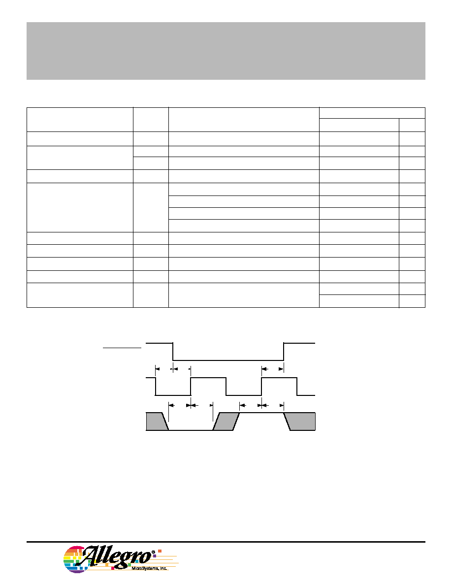
DATA
CLOCK
Dwg. WP-019
A
C
B
D
C
D
CHIP SELECT
E
A.
Minimum CHIP SELECT setup time before CLOCK rising edge .......... 100 ns
B.
Minimum CHIP SELECT hold time after CLOCK rising edge ............... 150 ns
C.
Minimum DATA setup time before CLOCK rising edge ........................ 150 ns
D.
Minimum DATA hold time after CLOCK rising edge ............................. 150 ns
E.
Minimum CLOCK low time before CHIP SELECT .................................. 50 ns
F.
Maximum CLOCK frequency .............................................................. 3.3 MHz

8902≠A
3-PHASE BRUSHLESS DC
MOTOR CONTROLLER/DRIVER
TERMINAL FUNCTIONS
Term.
Terminal Name
Function
1
LOAD SUPPLY
V
BB
; the 5 V or 12 V motor supply.
2
C
D2
One of two capacitors used to generate the ideal commutation points from the
back-EMF zero crossing points.
3
C
WD
Timing capacitor used by the watchdog circuit to disable the back-EMF compara-
tors during commutation transients, and to detect incorrect motor position.
4
C
ST
Startup oscillator timing capacitor.
5
OUT
A
Power amplifier A output to motor.
6-7
GROUND
Power and logic ground and thermal heat sink.
8
OUT
B
Power amplifier B output to motor.
9
OUT
C
Power amplifier C output to motor.
10
CENTERTAP
Motor centertap connection for back-EMF detection circuitry.
11
BRAKE
Active low turns ON all three sink drivers shorting the motor windings to ground.
External capacitor and resistor at B
RAKE
provide brake delay. The brake function
can also be controlled via the serial port.
12
C
RES
External reservoir capacitor used to hold charge to drive the source drivers'
gates. Also provides power for brake circuit.
13
FILTER
Analog voltage input to control motor current. Also, compensation node for
internal speed control loop.
14
SECTOR DATA
External tachometer input. Can use sector or index pulses from disk to provide
precise motor speed feedback to internal frequency-locked loop.
15
LOGIC SUPPLY
V
DD
; the 5 V logic supply.
16
OSCILLATOR
Clock input for the speed reference counter. Typical max. frequency is 10 MHz.
17
DATA OUT
Thermal shutdown indicator, FCOM, TACH, or SYNC signals available in real
time, controlled by 2-bit multiplexer in serial port.
18-19
GROUND
Power and logic ground and thermal heat sink.
20
RESET
When pulled low forces the chip into sleep mode; clears all serial port bits.
21
CHIP SELECT
Strobe input (active low) for data word.
22
CLOCK
Clock input for serial port.
23
DATA IN
Sequential data input for the serial port.
24
C
D1
One of two capacitors used to generate the ideal commutation points from the
back-EMF zero crossing points.