Äîêóìåíòàöèÿ è îïèñàíèÿ www.docs.chipfind.ru
Current Sensor: ACS755xCB-050
115 Northeast Cutoff, Box 15036
Worcester, Massachusetts 01615-0036 (508) 853-5000
ACS755050-DS, Rev. 2
5
4
3
2
1
Pin 1: VCC
Pin 2: GND
Pin 3: VOUT
Terminal 4: IP+
Terminal 5: IP
5
4
3
2
1
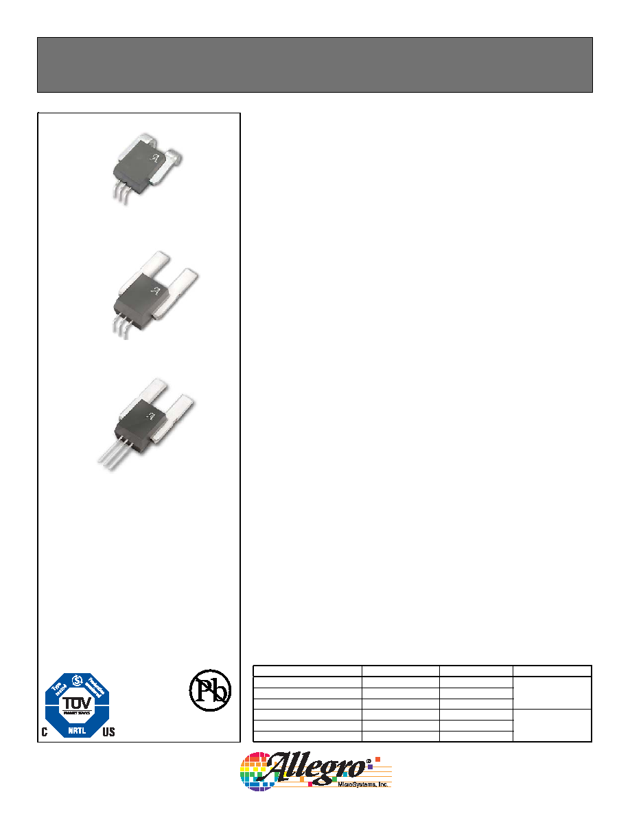
Package CB-PSF
5
4
3
2
1
Package CB-PSS
AB SO LUTE MAX I MUM RAT INGS
Supply Voltage, V
CC
..........................................16 V
Reverse Supply Voltage, V
RCC
........................16 V
Output Voltage, V
OUT
........................................16 V
Reverse Output Voltage, V
ROUT
...................... 0.1 V
Output Current Source, I
OUT(Source)
................. 3 mA
Output Current Sink, I
OUT(Sink)
.......................10 mA
Operating Temperature,
Ambient,
T
A
, L range ..................... 40 to 150ºC
Ambient,
T
A
, S range ....................... 20 to 85ºC
Maximum Junction, T
J(max)
............................. 165°C
Maximum Storage Temperature, T
S
....65 to 170°C
Package CB-PFF
Use the following complete part numbers when ordering:
Features and Benefi ts
· Monolithic Hall IC for high reliability
· Single +5 V supply
· 3
kV
RMS
isolation voltage between terminals 4/5 and pins 1/2/3
· 18 kHz bandwidth
· Automotive temperature range
· End-of-line factory-trimmed for gain and offset
· Ultra-low power loss: 100 internal conductor resistance
· Ratiometric output from supply voltage
· Extremely stable output offset voltage
· Small package size, with easy mounting capability
· Output proportional to ac and dc currents
Applications
· Automotive
systems
· Industrial
systems
· Power
conversion
· Battery
monitors
Part Number
Signal Pins
Terminals
Ambient
ACS755LCB-050-PFF
Formed
Formed
40 to 150°C
ACS755LCB-050-PSF
Formed
Straight
ACS755LCB-050-PSS
Straight
Straight
ACS755SCB-050-PFF
Formed
Formed
20 to 85°C
ACS755SCB-050-PSF
Formed
Straight
ACS755SCB-050-PSS
Straight
Straight
TÜV America
Certifi cate Number:
U8V 04 11 54214 001
The Allegro ACS75x family of current sensors provides economical and
precise solutions for current sensing in industrial, automotive, commercial, and
communications systems. The device package allows for easy implementation by
the customer. Typical applications include load detection and management, power
supplies, and overcurrent fault protection.
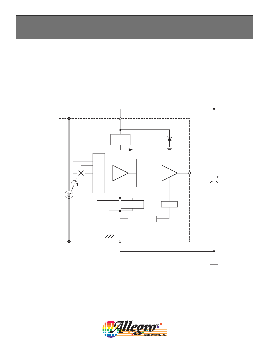
The device consists of a precision, low-offset linear Hall sensor circuit with a
copper conduction path located near the die. Applied current fl owing through
this copper conduction path generates a magnetic fi eld which is sensed by the
integrated Hall IC and converted into a proportional voltage. Device accuracy
is optimized through the close proximity of the magnetic signal to the Hall
transducer. A precise, proportional voltage is provided by the low-offset, chopper-
stabilized BiCMOS Hall IC, which is programmed for accuracy at the factory.
The output of the device will be valid when the current fl ows from pin 4 to pin 5.
The internal resistance of this conductive path is typically 100 , providing
low power loss. The thickness of the copper conductor allows survival of the
device at up to 5× overcurrent conditions. The terminals of the conductive path
are electrically isolated from the sensor leads (pins 1 through 3). This allows the
ACS75x family of sensors to be used in applications requiring electrical isolation
without the use of opto-isolators or other costly isolation techniques.
The device is fully calibrated prior to shipment from the factory. The ACS75x
family is lead-free. All leads are coated with 100% matte tin, and there is no lead
inside the package. The heavy gauge leadframe is made of oxygen-free copper.
2
115 Northeast Cutoff, Box 15036
Worcester, Massachusetts 01615-0036 (508) 853-5000
ACS755050-DS, Rev. 2
Current Sensor: ACS755xCB-050
Amp
Out
VCC
+5 V
Pin 1
Pin 3
VOUT
GND
Pin 2
Filter
Dynamic Of
fset
Cancellation
0.1 F
IP
IP+
Gain
Temperature
Coefficient
Offset
Voltage
Regulator
Trim Control
To all subcircuits
Terminal 5
Terminal 4
Functional Block Diagram

3
115 Northeast Cutoff, Box 15036
Worcester, Massachusetts 01615-0036 (508) 853-5000
ACS755050-DS, Rev. 2
Current Sensor: ACS755xCB-050
Characteristic
Symbol
Test Conditions
Min.
Typ.
Max.
Units
Primary Sensed Current
I
P
0
50
A
Supply Voltage
V
CC
4.5
5.0
5.5
V
Supply Current
I
CC
V
CC
= 5.0 V, output open
6.5
8
10
mA
Output Resistance
R
OUT
I
OUT
= 1.2 mA
1
2
Output Capacitance Load
C
LOAD
VOUT to GND
10
nF
Output Resistive Load
R
LOAD
VOUT to GND
4.7
k
Primary Conductor Resistance
R
PRIMARY
I
P
= +100A; T
A
= 25°C
100
Isolation Voltage
V
ISO
Pins 1-3 and 4-5; 60 Hz, 1 minute
3.0
kV
PERFORMANCE CHARACTERISTICS, -20°C to +85°C
, V
CC
= 5 V unless otherwise specifi ed
Propagation time
t
PROP
I
P
= +50 A, T
A
= 25°C
4
s
Response time
t
RESPONSE
I
P
= +50 A, T
A
= 25°C
20
s
Rise time
t
r
I
P
= +50 A, T
A
= 25°C
20
s
Frequency Bandwidth
f
3 dB , T
A
= 25°C
18
kHz
Sensitivity
Sens
Over full range of I
P
, T
A
= 25°C
60
mV/A
Over full range of I
P
53
65
mV/A
Noise
V
NOISE
Peak-to-peak, T
A
= 25°C,
no external fi lter
85
mV
Linearity
E
LIN
Over full range of I
P
±2.8
%
Zero Current Output Voltage
V
OUT(Q)
I = 0 A, T
A
= 25°C
0.6
V
Electrical Offset Voltage
(Magnetic error not included)
V
OE
I = 0 A, T
A
= 25°C
15
15
mV
I = 0 A
25
25
mV
Magnetic Offset Error
I
ERROM
I = 0 A, after excursion of 100 A
±0.1
±0.15
A
Total Output Error
(Including all offsets)
E
TOT
Over full range of I
P
, T
A
= 25°C
±1.0
%
Over full range of I
P
±10.0
%
PERFORMANCE CHARACTERISTICS, -40°C to +150°C
, V
CC
= 5 V unless otherwise specifi ed
Propagation time
t
PROP
I
P
= +50 A, T
A
= 25°C
4
s
Response time
t
RESPONSE
I
P
= +50 A, T
A
= 25°C
20
s
Rise time
t
r
I
P
= +50 A, T
A
= 25°C
20
s
Frequency Bandwidth
f
3 dB , T
A
= 25°C
18
kHz
Sensitivity
Sens
Over full range of I
P
, T
A
= 25°C
60
mV/A
Over full range of I
P
53
65
mV/A
Noise
V
NOISE
Peak-to-peak, T
A
= 25°C,
no external fi lter
85
mV
Linearity
E
LIN
Over full range of I
P
±2.8
%
Zero Current Output Voltage
V
OUT(Q)
I = 0 A, T
A
= 25°C
0.6
V
Electrical Offset Voltage
(Magnetic error not included)
V
OE
I = 0 A, T
A
= 25°C
15
15
mV
I = 0 A
50
50
mV
Magnetic Offset Error
I
ERROM
I = 0 A, after excursion of 100 A
±0.1
±0.15
A
Total Output Error
(Including all offsets)
E
TOT
Over full range of I
P
, T
A
= 25°C
±1.0
%
Over full range of I
P
±11.0
%
ELECTRICAL CHARACTERISTICS,
over operating ambient temperature range unless otherwise stated

4
115 Northeast Cutoff, Box 15036
Worcester, Massachusetts 01615-0036 (508) 853-5000
ACS755050-DS, Rev. 2
Current Sensor: ACS755xCB-050
Sensitivity (Sens): The change in sensor output in response to a 1 A change through the primary conductor. The sensitivity is the
product of the magnetic circuit sensitivity (G / A) and the linear IC amplifi er gain (mV/G). The linear IC amplifi er gain is trimmed at the
factory to optimize the sensitivity (mV/A) for the full-scale current of the device.
Noise (V
NOISE
): The product of the linear IC amplifi er gain (mV/G) and the noise fl oor for the Allegro Hall effect linear IC (1 G).
The noise fl oor is derived from the thermal and shot noise observed in Hall elements. Dividing the noise (mV) by the sensitivity
(mV/A) provides the smallest current that the device is able to resolve.
Linearity (E
LIN
): The degree to which the voltage output from the sensor varies in direct proportion to the primary current through its
full-scale amplitude. Nonlinearity in the output can be attributed to the saturation of the fl ux concentrator approaching the full-scale
current. The following equation is used to derive the linearity
Defi nitions of Accuracy Characteristics
where
Vout_¼ full-scale I
P
(V) is the output voltage when the sensed current approximates 0.25
× I
P(max)
, and
Vout_¾ full-scale I
P
(V) is the output voltage when the sensed current approximates 0.75
× I
P(max)
.
Quiescent output voltage (V
OUT(Q)
): The output of the sensor when the primary current is zero. For a unipolar supply voltage, it
nominally remains at 0.6 V. Variation in V
OUT(Q)
can be attributed to the resolution of the Allegro linear IC quiescent voltage trim,
magnetic hysteresis, and thermal drift.
Electrical offset voltage (V
OE
): The deviation of the device output from its ideal quiescent value due to nonmagnetic causes.
Magnetic offset error (I
ERROM
): The magnetic offset is due to the residual magnetism (remnant fi eld) of the core material. The mag-
netic offset error is highest when the magnetic circuit has been saturated, usually when the device has been subjected to a full-scale or
high-current overload condition. The magnetic offset is largely dependent on the material used as a fl ux concentrator. The larger mag-
netic offsets are observed at the lower operating temperatures.
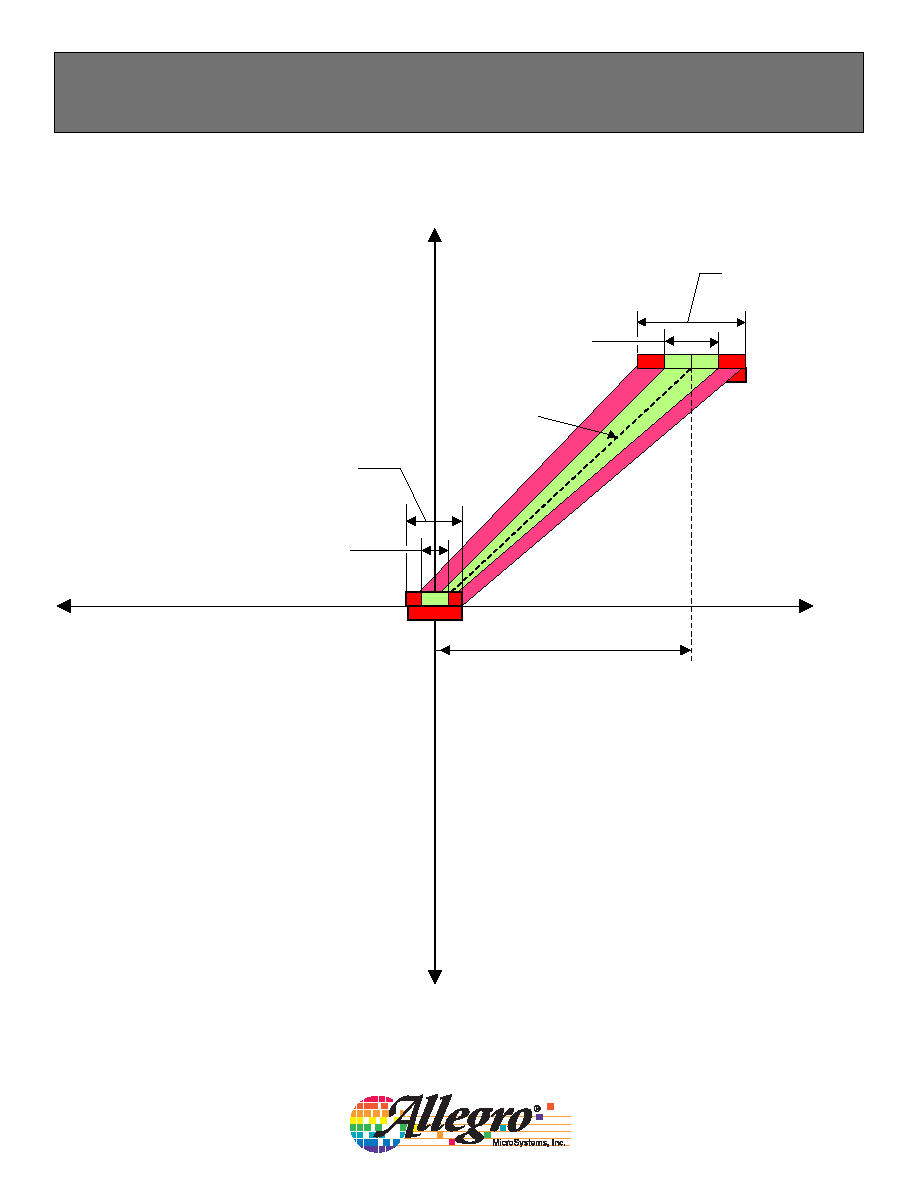
Accuracy (E
TOT
): The accuracy represents the maximum deviation of the actual output from its ideal value. This is also known as the
total ouput error. The accuracy is illustrated graphically in the Output Voltage versus Current chart on the following page.
Accuracy is divided into four areas:
· 0 A at 25°C: Accuracy of sensing zero current fl ow at 25°C, without the effects of temperature.
· 0 A over temperature: Accuracy of sensing zero current fl ow including temperature effects.
· Full-scale current at 25°C: Accuracy of sensing the full-scale current at 25°C, without the effects of temperature.
· Full-scale current over temperature: Accuracy of sensing full-scale current fl ow including temperature effects.
Nonlinearity (%) = 100
1
Vout _
1
/
4
full-scale I
P
V
OUT(Q)
Vout _
3
/
4
full-scale I
P
V
OUT(Q)
3
5
115 Northeast Cutoff, Box 15036
Worcester, Massachusetts 01615-0036 (508) 853-5000
ACS755050-DS, Rev. 2
Current Sensor: ACS755xCB-050
Increasing V
OUT
(V)
+I
P
(A)
Accuracy
Accuracy
25°C Only
Accuracy
25°C Only
Accuracy
0 A
v r
O e Temperature
Average
V
OUT
I
P
(A)
v r
O e Temperature
Decreasing V
OUT
(V)
50 A
Full Scale
Output voltage vs. current, illustrating sensor accuracy at 0 A and at full-scale current