Programmable Back Biased Hall-Effect
Switch with TPOS Functionality
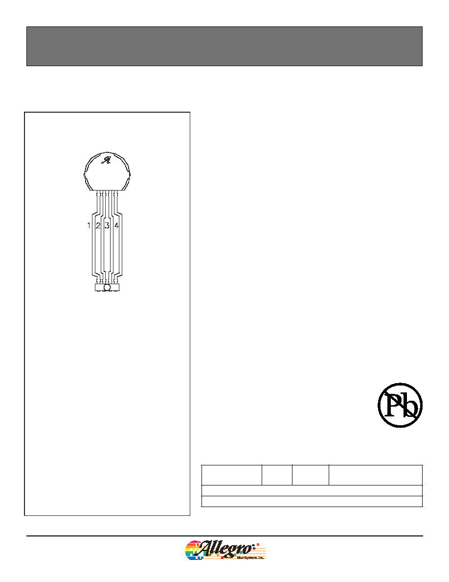
PACKAGE DIAGRAM
Pin 1 = VCC
Pin 2 = VOUT
Pin 3 = No Connect
Pin 4 = GND
The ATS635LSE and ATS636LSE programmable, true power-on state
(TPOS), sensors are an optimized Hall-effect IC and magnet combination
that switch in response to magnetic signals created by ferrous targets in
gear-tooth sensing and proximity applications.
The devices are externally programmable.
A wide range of
programmability is available on the magnetic operate point (B
OP
) while the
hysteresis remains fixed. This advanced feature allows for optimization of
the sensor switch point and can drastically reduce the effects of
mechanical placement tolerances found in production environments
.
A proprietary dynamic offset cancellation technique, with an internal
high-frequency clock, reduces the residual offset voltage, which is normally
caused by device overmolding, temperature dependencies, and thermal
stress. Having the Hall element and amplifier in a single chip minimizes
many problems normally associated with low-level analog signals.
This sensor system is ideal for use in gathering speed or position
information using gear-tooth-based configurations, or for proximity sensing
with ferrous targets.
The ATS635LSE switches HIGH in the presence of a ferrous target or
tooth and switches LOW in the presence of a target valley, window, or
when the ferrous target is removed. The ATS636LSE has the opposite
polarity and switches LOW in the presence of a ferrous target or tooth and
switches HIGH in the presence of a target valley, window, or when the
ferrous target is removed.
ABSOLUTE MAXIMUM RATINGS
Supply Voltage, V
CC
.............................. 28 V*
Reverse Supply Voltage, V
RCC
............... -18 V
Overvoltage Supply Current, I
CC
...........100 mA
Output Off Voltage, V
OUT......
.................. 26.5V
Output Sink Current, I
OUT
................... 20 mA
Magnetic Flux Density, B............... Unlimited
Package Power Dissipation, P
D
..... See Graph
Operating Temperature Range, T
A
Suffix "L"....................... -40 �C to +150 �C
Junction Temperature, T
J
......................165 �C
Storage Temperature Range
T
S
.............................. -65 �C to +170 �C
*Fault conditions that produce supply voltage transients will
be clamped by an internal Zener diode. These conditions
can be tolerated but should be avoided.
Internal current limiting is intended to protect the device
from output short circuits, but is not intended for continuous
operation.
FEATURES
Chopper Stabilization
Extremely low switch-point drift over temperature
On-chip Protection
Supply transient protection
Output short-circuit protection
Reverse-battery protection
True Zero-Speed Operation
True Power-On State
Single-chip Sensing IC for High Reliability
Optimized Magnetic Circuit
Wide Operating Voltage Range
Internal Regulator
These devices are available in lead (Pb) free versions, with 100%
matte tin leadframe plating.
ATS635LSE and ATS636LSE
ATS635LSE-DS
Worcester, Massachusetts 01615-0036 (508) 853-5000
115 Northeast Cutoff, Box 15036
www.allegromicro.com
Allegro MicroSystems, Inc.
Use the following complete part numbers when ordering:
Part Number
Pb-Free
Output
(Tooth)
Packing*
ATS635LSETN-T
Yes
High
13-in. reel, 450 pieces/reel
ATS636LSETN-T
Yes
Low
13-in. reel, 450 pieces/reel
*Contact Allegro for additional packing options.

ATS635LSE and ATS636LSE
PROGRAMMABLE TRUE POWER-ON HALL-EFFECT GEAR-TOOTH SWITCHES
Page 2 of 15
115 Northeast Cutoff, Box 15036
Worcester, Massachusetts 01615-0036 (508) 853-5000
Copyright � 2005 Allegro MicroSystems, Inc.
CHARACTERISTICS
ELECTRICAL CHARACTERISTICS over operating voltage and junction temperature range
(unless otherwise noted)
Limits
Characteristics
Symbol
Test Conditions
Min.
Typ.
Max.
Units
Supply Voltage
1
V
CC
Operating
4.2
�
24
V
After programming
V
CC
= 0 � V
CC(min)
, t > t
ON
:
B < B
OP
ATS636
HIGH
HIGH
HIGH
�
Power-Up State
POS
B < B
OP
ATS635
LOW
LOW
LOW
�
Low Output Voltage
V
OUT(SAT)
Output on, I
OUT
= 20 mA
�
175
400
mV
Output Current Limit
2
I
OUTM
Pulse test method
Output on
30
50
90
mA
Output Leakage Current
I
OFF
Output off, V
OUT
= 24 V
�
�
10
�A
Output off (HIGH)
�
2.5
5.5
mA
Supply Current
I
CC
Output on (LOW)
�
2.5
5.5
mA
Reverse Supply Current
I
RCC
V
RCC
= -18V
�
�
-5
mA
Power-On Delay
3
t
ON
Output off; V
CC
> V
CC(min)
�
35
50
�s
Output Rise Time
t
r
R
L
= 820 , C
L
= 10 pF
�
1.2
5
�s
Output Fall Time
t
f
R
L
= 820 , C
L
= 10 pF
�
1.2
5
�s
Sampling Frequency
f
Sample
-
�
250
-
kHz
Supply Zener Voltage
V
Zsupply
I
CC
= I
CC(max)
+ 3 mA
T
A
= 25�C
28
�
�
V
Output Zener Voltage
V
ZOutput
I
OUT
= 3 mA
T
A
= 25�C
30
�
�
V
Supply Zener Current
4
I
Zsupply
V
S
= 28 V
�
�
8.5
mA
Output Zener Current
I
ZOutput
V
O
= 30 V
�
�
3
mA
Note: Typical data is at V
CC
= 12 V and T
A
= +25�C.
1
Do not exceed the maximum thermal junction temperature: see power de-rating curve.
2
Short circuit protection is not intended for continuous operation and is tested using pulses.
3
The power on delay is the time that is necessary before the output signal is valid
4
The maximum spec limit for this parameter is equivalent to
I
CC(max)
+ 3 mA
ATS635LSE and ATS636LSE
PROGRAMMABLE TRUE POWER-ON HALL-EFFECT GEAR-TOOTH SWITCHES
115 Northeast Cutoff, Box 15036
Worcester, Massachusetts 01615-0036 (508) 853-5000
Copyright � 2005 Allegro MicroSystems, Inc.
MAGNETIC CHARACTERISTICS over operating voltage and junction temperature range using
reference target (Unless otherwise noted)
Limits
Characteristics
Symbol
Test Conditions
Min.
Typ.
Max.
Units
Switch Point
�
7
�
Bit
Switch Point Polarity
�
1
�
Bit
Number of Programming
Bits
-
Programming Lock
�
1
�
Bit
Gear Tooth Sensor / Proximity Sensing Characteristics (Low Switchpoint Only)
Temp: 25�C Code �127
2.5
�
�
mm
1
Programming Air Gap
Range
AG
Range
Temp: 25�C Code +127
�
�
1.5
mm
Programming Resolution
AG
Res
Temperature: 25�C
Program Air Gap = 2.5 mm
�
0.05
�
mm
2
Air Gap Drift Over Full
Temperature Range
AG
Drift
Device Programmed
to 2.5 mm
�
0.2
�
mm
Over Tooth
(ATS635LSE)
�
HIGH
�
�
Over Valley
(ATS635LSE)
�
LOW
�
�
Over Tooth
(ATS636LSE)
�
LOW
�
�
Polarity
P
Over Valley
(ATS636LSE)
�
HIGH
�
�
1
The switch point will vary over temperature. A sufficient margin obtained through customer testing is required to guarantee functionality over
temperature. Programming at larger air gaps leaves no safety margin for switchpoint drift. See the applications note: "Proximity Sensing
Programming Technique"
http://www.allegromicro.com/techpub2/proximity_sensing/
or visit the Allegro website at
http://www.allegromicro.com
for additional information.
2
The switch point will vary over temperature, proportionally to the programmed air gap. This parameter is based on characterization data and is not
a tested parameter in production. Switch point air gap generally drifts downward as temperature increases.
Tooth and Valley Field vs. Air Gap
Reference Target
0
200
400
600
800
1000
1200
1400
0.0
0.5
1.0
1.5
2.0
2.5
3.0
3.5
4.0
4.5
5.0
5.5
6.0
Air Gap [mm]
Flux Density [Gauss]
Reference Target Tooth
Reference Target Valley
Reference Target Tooth and Valley Field vs. Air Gap
Reference Target Flux Density vs. Position
0
200
400
600
800
1000
1200
1400
0
30
60
90 120 150 180 210 240 270 300 330 360
Position (�)
Flux Density (Gauss)
0.25
0.50
0.75
1.00
1.25
1.50
1.75
2.00
2.25
2.50
2.75
3.00
3.25
3.50
3.75
4.00
4.25
4.50
4.75
5.00
5.25
5.50
5.75
6.00
Reference Target Flux Density vs. Position: Typical
ATS635LSE and ATS636LSE
PROGRAMMABLE TRUE POWER-ON HALL-EFFECT GEAR-TOOTH SWITCHES
115 Northeast Cutoff, Box 15036
Worcester, Massachusetts 01615-0036 (508) 853-5000
Copyright � 2005 Allegro MicroSystems, Inc.
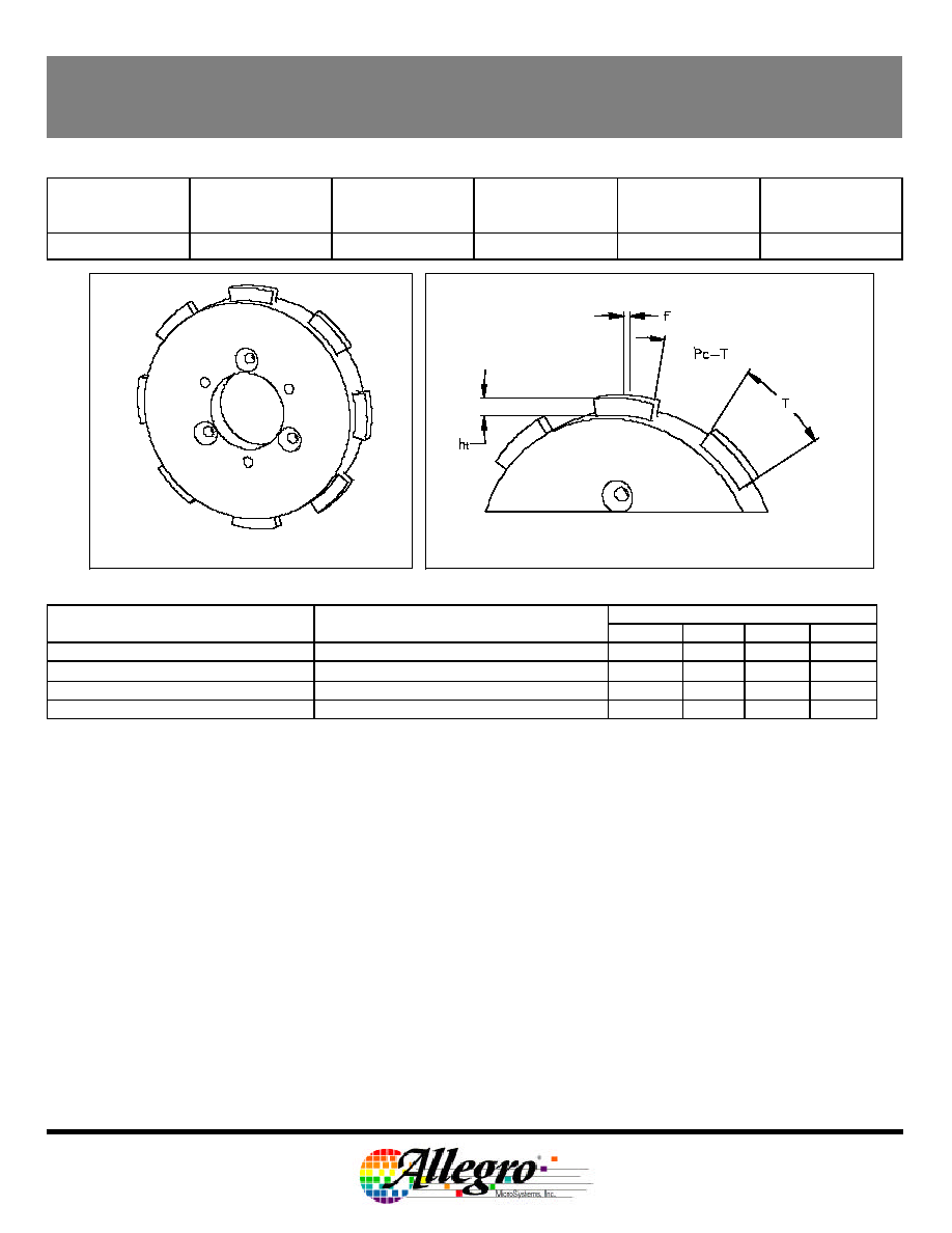
REFERENCE TARGET DIMENSIONS
Target
Outside
Diameter
(D
o
)
Face Width
(F)
Circular Tooth
Length
(T)
Circular Valley
Length
(P
C
� T)
Tooth Whole
Depth
(h
t
)
Reference Target
120mm
6mm
23.5mm
23.5mm
5mm
GEAR PARAMETERS FOR CORRECT OPERATION
Limits
Characteristic
Description
Min.
Typ.
Max.
Units
Tooth Whole Depth
(h
t
)
Depth of Target Valley
5
�
�
mm
Circular Valley Length
(P
C
� T)
Length of Target Valley
13
�
�
mm
Circular Tooth Length
(T)
Length of Target Tooth
5
�
�
mm
Face Width
(F)
Thickness or Width of Target Tooth
5
�
�
mm
MATERIAL:
CRS 1018
Reference Target
Reference Target
ATS635LSE and ATS636LSE
PROGRAMMABLE TRUE POWER-ON HALL-EFFECT GEAR-TOOTH SWITCHES
115 Northeast Cutoff, Box 15036
Worcester, Massachusetts 01615-0036 (508) 853-5000
Copyright � 2005 Allegro MicroSystems, Inc.
ELECTROMAGNETC CAPABILITY (EMC) PERFORMANCE
Please contact Allegro MicroSystems for EMC performance
Test Name
Reference Specification
ESD � Human Body Model
AEC-Q100-002
ESD � Machine Model
AEC-Q100-003
Conducted Transients
ISO 7637-1
Direct RF Injection
ISO 11452-7
Bulk Current Injection
ISO 11452-4
TEM Cell
ISO 11452-3
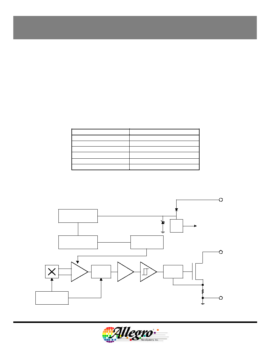
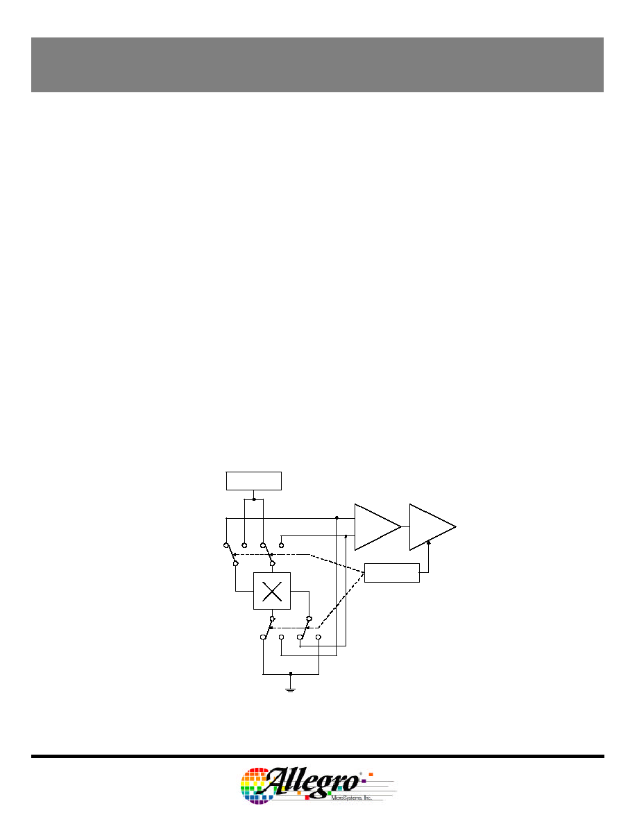
FUNCTIONAL BLOCK DIAGRAM
Reg
Clock/Logic
AMP
S/H
LPF
Current
Limit
VCC
OUT
GND
Programmming
Logic
Program / Lock
Offset Adjust
To all
subcircuits
ATS635LSE and ATS636LSE
PROGRAMMABLE TRUE POWER-ON HALL-EFFECT GEAR-TOOTH SWITCHES
115 Northeast Cutoff, Box 15036
Worcester, Massachusetts 01615-0036 (508) 853-5000
Copyright � 2005 Allegro MicroSystems, Inc.
Regulator
Amplifier
Sample/
Hold
CLOCK
Hall Element
FUNCTIONAL DESCRIPTION
Chopper-Stabilized Technique
.
The basic Hall sensor
is a small sheet of semiconductor material in which a
constant bias current will flow when a constant voltage
source is applied. The output will take the form of a
voltage measured across the width of the sheet and will
have negligible value in the absence of a magnetic field.
When a magnetic field with flux lines at right angles to
the Hall current is applied, a small signal voltage directly
proportional to the strength of the magnetic field will
occur at the output terminals.
This signal voltage is proportionally small relative to the
offset produced at the input of the chip. This makes it
very difficult to process the signal and maintain an
accurate, reliable output over the specified temperature
and voltage range. Therefore, it is important to reduce
any offset on the signal that could be amplified when the
signal is processed.
Chopper Stabilization is a unique approach used to
minimize input offset on the chip. This technique
removes a key source of output drift with temperature
and stress, and produces a 3X reduction in offset over
other conventional methods.
This offset reduction Chopping Technique is based on a
signal modulation-demodulation process. The undesired
offset signal is separated from the magnetically induced
signal in the frequency domain. The offset (and any low
frequency noise) component of the signal can be seen
as signal corruption added after the signal modulation
process has taken place. Therefore, the DC offset is not
modulated and remains a low frequency component.
Consequently, the signal demodulation process acts as
a modulation process for the offset causing the
magnetically induced signal to recover its original
spectrum at baseband while the DC offset becomes a
high frequency signal. Then, using a low pass filter the
signal passes while the modulated DC offset is
suppressed.
The advantage of this approach is significant offset
reduction, which de-sensitizes the chip against the
effects of temperature and stress. The disadvantage is
that this technique features a demodulator that uses a
sample and hold block to store and recover the signal.
This sampling process can slightly degrade the Signal-
to-Noise Ratio (SNR) by producing replicas of the noise
spectrum at the baseband. The degradation is a
function of the ratio between the white noise spectrum
and the sampling frequency. The effect of the
degradation of the SNR is higher jitter, a.k.a. signal
repeatability. In comparison to a continuous time device,
the jitter spec can be increased by a factor of five.
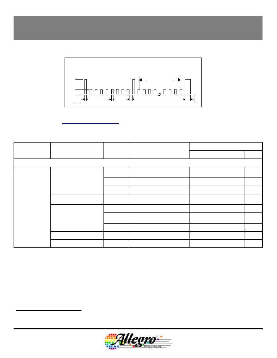
Figure 1 � Concept of Chopper-Stabilization Algorithm

ATS635LSE and ATS636LSE
PROGRAMMABLE TRUE POWER-ON HALL-EFFECT GEAR-TOOTH SWITCHES
Page 7 of 15
115 Northeast Cutoff, Box 15036
Worcester, Massachusetts 01615-0036 (508) 853-5000
Copyright � 2005 Allegro MicroSystems, Inc.
FUNCTION DESCRIPTION: ADDRESSING / PROGRAMMING PROTOCOL
The ATS635LSE and ATS636LSE magnetic operate point (B
OP
) is programmed by serially addressing the devices
through the supply terminal (1). After the correct operate point is determined, the device programming bits are selected
and blown, then a lock bit is selected and blown to prevent any further (accidental) programming.
Addressing:
Bop is programmable in both the positive and negative direction from its initial value. Addressing is used to
determine the desired code, while programming is used to lock the code. A unique key is needed to blow fuses, while
addressing as described below does not allow for the device to be programmed accidentally.
Addressing with positive polarity.
The magnetic operate point (B
OP
) is adjustable using 7 bits or 128 addresses. The
Addresses are sequentially selected (Figure 2) until the required operate point is reached. The first address must be
selected with a High voltage pulse (V
PP
), while the remaining pulses should be V
PH
Pulses. Note that the difference
between B
OP
and the magnetic release point (B
RP
), the Hysteresis (B
HYS
), is fixed for all addresses.
0
V
PL
V
PH
t
d(1)
t
d(0)
Code 1
Code 2
Code 3
Code N-2
Code N-1
Code N
(Up to 127)
V
PP
Figure 2 � Addressing Pulses: Positive Polarity
Addressing with negative polarity.
The magnetic operate point (B
OP
) is adjustable with negative polarity using 7 bits or
128 addresses. To invert the polarity it is necessary to first apply a keying sequence (Figure 3). Th e polarity key contains
a V
PP
pulse and at least 1 V
PH
pulse, but no more than 6 V
PH
pulses; the key in Figure 3 shows 2 V
PH
pulses. The
addresses are then sequentially selected until the required operate point is reached. The first address must be selected
with a High voltage pulse (V
PP
), while the remaining pulses should be V
PH
Pulses.
0
V
PP
V
PL
V
PH
t
d(1)
t
d(0)
Code -1
Code -2
Code -3
Code -(N-2)
Code -(N-1)
Code -N
(Up to -127)
Polarity
Key
Figure 3 � Addressing Pulses: Negative Polarity

ATS635LSE and ATS636LSE
PROGRAMMABLE TRUE POWER-ON HALL-EFFECT GEAR-TOOTH SWITCHES
Page 8 of 15
115 Northeast Cutoff, Box 15036
Worcester, Massachusetts 01615-0036 (508) 853-5000
Copyright � 2005 Allegro MicroSystems, Inc.
Program Enable.
To program the device, a keying sequence is used to activate / enable the programming mode as
shown in Figure 4. This program key sequence consisting of a V
PP
pulse, at least seven V
PH
pulses, and a V
PP
pulse with
no supply interruptions. The sequence is designed to prevent the device from being programmed accidentally (e.g., as a
result of noise on the supply line).
0
t
d(1)
t
d(1)
t
d(0)
PROGRAM ENABLE
7 or More Pulses
(8 Pulses Shown)
V
PL
V
PH
V
PP
Figure 4 � Program Enable Pulse Sequence
Code Programming.
After the desired switch point code is selected (0 through 127), each bit of the corresponding binary
address should be programmed individually, not at the same time. For example, to program code 5 (binary 000101), bits
1 and 3 need to be programmed. A bit is programmed by addressing the code and then applying a V
PP
pulse, the
programming is not reversible. An appropriate sequence for blowing code 5 is shown in Figure 5.
Figure 5 � Code Programming Example
Polarity Bit Programming.
If the desired switchpoint has negative polarity, the polarity bit must be programmed. To do
this it is necessary to first apply the polarity key sequence before the program key sequence (Figure 6). Finally a V
PP
pulse of duration t
dP
must be applied to program this bit, the programming is not reversible. The polarity bit is for adjusting
programming range only and will not affect the output polarity. The proper output polarity device is determined by
ordering the correct part number (ATS635 or ATS636), as they are different ICs.
V
PH
V
PP
Program Enable
0
V
PL
t
d(1)
t
d(1)
t
d(0)
t
dP
Polarity
Key
Polarity Bit
Program
Figure 6 � Polarity Bit Programming
V
PH
V
PP
Program Enable
Bit 1 Address
Bit 1 Program
Bit 3 Address
000100
Code 4
Bit 3 Program
Program Enable
0
V
PL
t
d(1)
t
d(1)
t
d(0)
t
dP
000001
Code 1
ATS635LSE and ATS636LSE
PROGRAMMABLE TRUE POWER-ON HALL-EFFECT GEAR-TOOTH SWITCHES
Page 9 of 15
115 Northeast Cutoff, Box 15036
Worcester, Massachusetts 01615-0036 (508) 853-5000
Copyright � 2005 Allegro MicroSystems, Inc.
Lock-Bit Programming.
After the desired code is programmed, the lock bit (code 128), can be programmed (figure 7) to
prevent further programming of the device. Again; programming is not reversible.
Figure 7 � Lock-Bit Programming Pulse Sequence
See Allegro website at
http://www.allegromicro.com
for extensive information on device programming as well as
programming products. Programming hardware is available for purchase and programming software is available for free.
Valid over operating temperature range unless otherwise noted
.
Limits
Part Number
Characteristics
Symbol
Test Conditions
Min.
Typ.
Max.
Units
PROGRAMMING PROTOCOL (T
A
= +25�C)
V
PL
Minimum voltage range
during programming
4.5
5
5.5
V
V
PH
8.5
�
15
V
5,6
Programming Voltage
V
PP
25
�
27
V
Programming Current
I
PP
Maximum supply current
during programming
�
500
�
mA
t
d(0)
OFF time between bits
20
�
�
�s
t
d(1)
Enable, address, program,
or lock bit ON time
20
�
�
�s
Pulsewidth
t
dP
Program pulse ON time
100
300
�
�s
Pulse Rise Time
t
r
V
PL
to V
PH
or V
PP
�
�
11
�s
ATS635 /
ATS636
Pulse Fall Time
t
f
V
PH
or V
PP
to V
PL
�
�
5
�s
5
Programming Voltages are measured at Pin 1 (V
CC
) of SIP. A minimum capacitance of 0.1 �F must be connected from V
CC
to GND
of the SIP to provide the current necessary to blow the fuse.
6
Testing is the only method that guarantees successful programming.
V
PH
V
PP
Program Enable
0
V
P L
t
d(1)
t
d(1)
t
d(0)
t
dP
Lock Bit
Address
128 Pulses
Lock Bit Program

ATS635LSE and ATS636LSE
PROGRAMMABLE TRUE POWER-ON HALL-EFFECT GEAR-TOOTH SWITCHES
115 Northeast Cutoff, Box 15036
Worcester, Massachusetts 01615-0036 (508) 853-5000
Copyright � 2005 Allegro MicroSystems, Inc.
FUNCTIONAL DESCRIPTION (CONT.): TYPICAL APPLICATION CIRCUIT
Applications. It is strongly recommended that an external ceramic bypass capacitor in the range of 0.01 �F to 0.1 �F be
connected between the supply and ground of the device to reduce both external noise and noise generated by the
chopper-stabilization technique. (The diagram below shows a 0.1 �F bypass capacitor.)
The series resistor R
S
in combination with the bypass capacitor creates a filter for EMC pulses. The series resistor will
have a drop of approximately 800 mV, this must be considered for the minimum V
CC
requirement of the ATS635LSE /
ATS636LSE. The small capacitor on the output of the device improves the EMC performance of the device.
The pull-up resistor should be chosen to limit the current through the output transistor; do not exceed the maximum
continuous output current of the device.
Note: This circuit cannot be used to program the device, as the series resistance is too large, and a minimum capacitance
of 0.1 �F must be connected from V
CC
to GND of the SIP to provide the current necessary to blow the fuse.
Typical Application:
1.2k Ohm
V
Supply
VCC
1
R
L
100 Ohm
2
4
GND
R
S
0.1 �F
5V
VOUT
ATS635/636
120 pF
Extensive applications information on magnets and Hall-effect sensors including Chopper-Stabilization is available in the
Allegro Electronic Data Book CD, or at the website:
http://www.allegromicro.com
.
ATS635LSE and ATS636LSE
PROGRAMMABLE TRUE POWER-ON HALL-EFFECT GEAR-TOOTH SWITCHES
Page 11 of 15
115 Northeast Cutoff, Box 15036
Worcester, Massachusetts 01615-0036 (508) 853-5000
Copyright � 2005 Allegro MicroSystems, Inc.
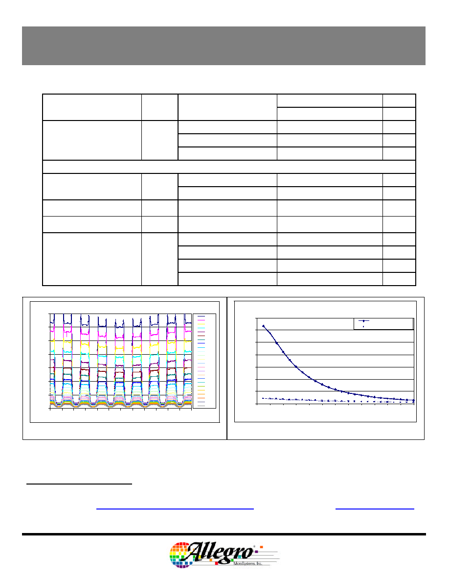
CHARACTERISTIC DATA
Data taken from 3 lots, 30 pieces/lot
Reference Target 8x
I
CC
ON
0
1
2
3
4
5
6
-50
-25
0
25
50
75
100
125
150
175
TEMPERATURE (�C)
I
CC
(mA)
4V
15V
24V
I
CC
OFF
0
1
2
3
4
5
6
-50
-25
0
25
50
75
100
125
150
175
TEMPERATURE (�C)
I
CC
(mA)
4V
15V
24V
V
SAT
0
100
200
300
400
500
-50
-25
0
25
50
75
100
125
150
175
TEMPERATURE (�C)
V
SAT
(mV)
20mA
ATS635LSE and ATS636LSE
PROGRAMMABLE TRUE POWER-ON HALL-EFFECT GEAR-TOOTH SWITCHES
Page 12 of 15
115 Northeast Cutoff, Box 15036
Worcester, Massachusetts 01615-0036 (508) 853-5000
Copyright � 2005 Allegro MicroSystems, Inc.
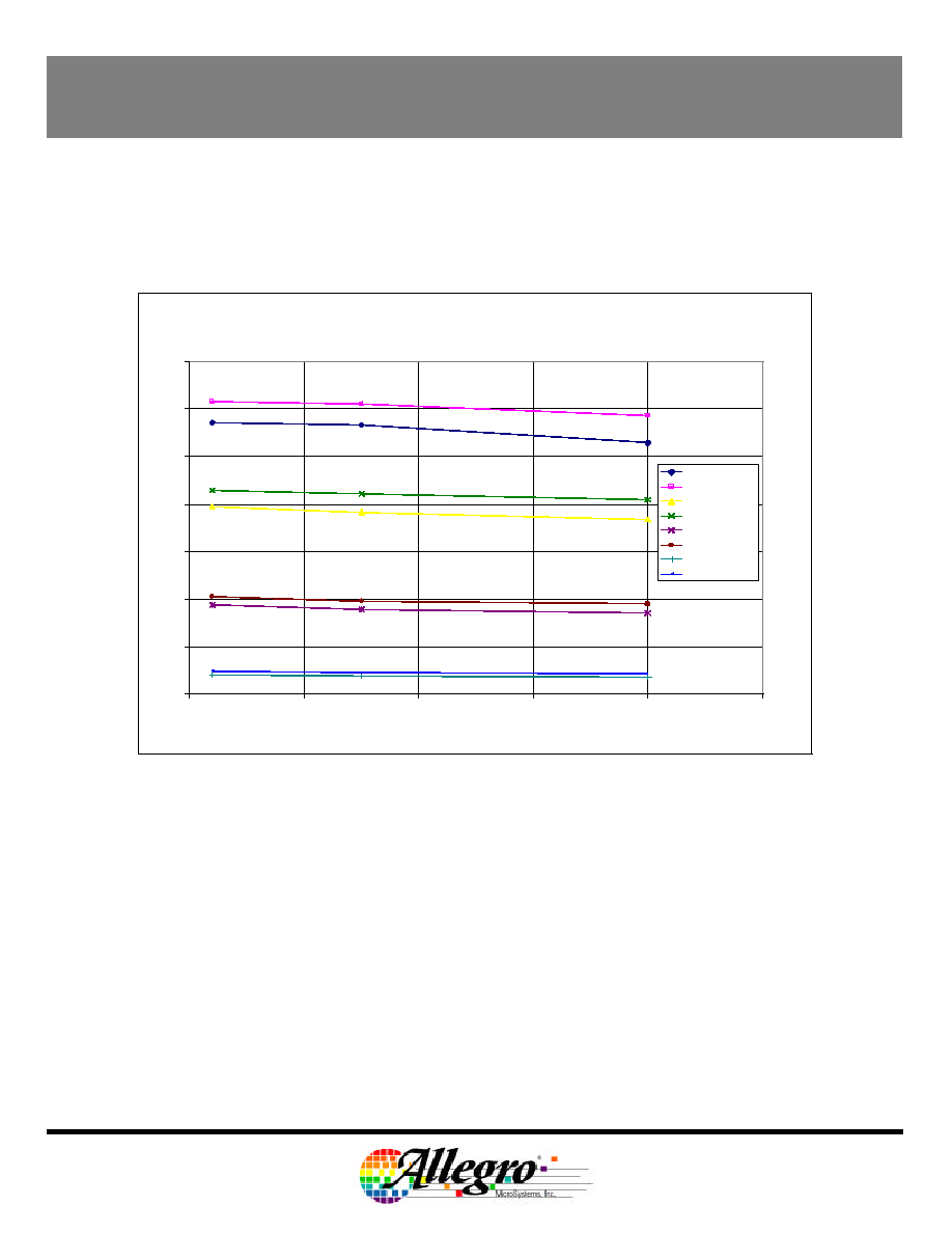
CHARACTERISTIC DATA (continued)
Data taken from 3 lots, 30 pieces/lot
Reference Target 8x
Notes:
s
Air gaps for Code 127 @ 150�C are interpolated due to test limitations at minimum air gap.
s
These graphs are intended to provide an understanding of how the program codes affect the switch points. In a
production environment, individual devices would be programmed to individual codes to ensure all devices switch at
the same air gap.
B
OP
/B
RP
vs. Program Code
0
1
2
3
4
5
6
7
-50
0
50
100
150
200
TEMPERATURE (�C)
AIR GAP (mm)
Code -8 BOP
Code -8 BRP
Code 0 BOP
Code 0 BRP
Code +32 BOP
Code +32 BRP
Code +127 BOP
Code +127 BRP
ATS635LSE and ATS636LSE
PROGRAMMABLE TRUE POWER-ON HALL-EFFECT GEAR-TOOTH SWITCHES
Page 13 of 15
115 Northeast Cutoff, Box 15036
Worcester, Massachusetts 01615-0036 (508) 853-5000
Copyright � 2005 Allegro MicroSystems, Inc.
POWER DE-RATING � SE Package
Power De -Rating
Due to internal power consumption, the temperature of the
IC (junction temperature, T
J
) is higher than the ambient
environment temperature, T
A
. To ensure that the device
does not operate above the maximum rated junction
temperature use the following calculations:
T=P
D
� R
JA
Where P
D
= V
CC
� I
CC
T = V
CC
� I
CC
� R
JA
Where T denotes the temperature rise resulting from the
IC's power dissipation:
T
J
= T
A
+ T
R
JA
= 77�C/W T
J(max)
= 165�C
Typical T
J
Calculation:
T
A
= 25�C, V
CC
= 5 V, I
CC(on)
= 5.5 mA
P
D
= V
CC
� I
CC
P
D
= 5 V � 5.5 mA = 27.5 mW
T = P
D
� R
JA
= 27.5 mW � 77�C/W = 2.0�
T
J
= T
A
+ T = 25�C + 2.0�C = 27.0�C
Maximum Allowable Power Dissipation Calculation
T
J
= T
A
+ T
T
J(max)
= 165�C, if T
A
= 150�C then:
165 = 150 + T
T = 15�C
DT = P
D
� R
JA
(R
JA
= 77�C/W)
\ P
D(max)
= 15�C / 77�C/W = 195 mW @ T
A
= 150�C
Maximum V
CC
for P
D(max)
=111 mW at T
A
=150�C
P
D
= V
CC
� I
CC
I
CC
= 10mA (max) at 150�C
V
CC
= P
D
/ I
CC
= 195 mW / 5.5 mA = 35.4 V
0
500
1000
1500
2000
2500
3000
3500
4000
4500
20
40
60
80
100
120
140
160
180
Temperature (�C)
Power D
i
s
s
i
p
a
t
i
o
n, P
D
(m
W)
Power Dissipation versus Ambient Temperature
(R
JA
= 77 �C/W)
2-layer PCB
ATS635LSE and ATS636LSE
PROGRAMMABLE TRUE POWER-ON HALL-EFFECT GEAR-TOOTH SWITCHES
Page 14 of 15
115 Northeast Cutoff, Box 15036
Worcester, Massachusetts 01615-0036 (508) 853-5000
Copyright � 2005 Allegro MicroSystems, Inc.
SE PACKAGE DIMENSIONS
Reference Dimensions Only
1.27 .050
1.08 .043
10 .394
7 .276
0.38 .015
6.2 .244
20.95 .825
11.6 .457
4.9 .193
3.3 .130
1.3 .051
2 .079
0.6 .240
2
4
3
1
A
A
A
B
C
C
D
D
B
Dambar removal protrusion (16X)
Metallic protrusion, electrically connected to pin 4 and substrate (both sides)
Active Area Depth, 0.43 mm [.017]
Thermoplastic Molded Lead Bar for alignment during shipment
E
Hall element (not to scale)
Preliminary dimensions, for reference only
Untoleranced dimensions are nominal.
Dimensions in millimeters
U.S. Customary dimensions (in.) in brackets, for reference only
Dimensions exclusive of mold flash, burrs, and dambar protrusions
Exact case and lead configuration at supplier discretion within limits shown
E

ATS635LSE and ATS636LSE
PROGRAMMABLE TRUE POWER-ON HALL-EFFECT GEAR-TOOTH SWITCHES
Page 15 of 15
115 Northeast Cutoff, Box 15036
Worcester, Massachusetts 01615-0036 (508) 853-5000
Copyright � 2005 Allegro MicroSystems, Inc.
The products described herein are manufactured under one or more
of the following U.S. patents: 5,045,920; 5,264,783; 5,442,283;
5,389,889; 5,581,179; 5,517,112; 5,619,137; 5,621,319; 5,650,719;
5,686,894; 5,694,038; 5,719,130; 5,917,320; and other patents pending.
Allegro MicroSystems, Inc. reserves the right to make, from time to
time, such departures from the detail specifications as may be required to
permit improvements in the design of its products. Before placing an
order, the user is cautioned to verify that the information being relied
upon is current.
Allegro products are not authorized for use as critical components in
life-support applications, devices, or systems without express written
approval.
The information included herein is believed to be accurate and
reliable. However, Allegro MicroSystems, Inc. assumes no responsibility
for its use; nor for any infringements of patents or other rights of third
parties which may result from its use.