© 2005 California Micro Devices Corp. All rights reserved.
11/08/05
490 N. McCarthy Blvd., Milpitas, CA 95035-5112
Tel: 408.263.3214
Fax: 408.263.7846
www.cmd.com
1
CM1440
6 Channel EMI Filter Array with ESD Protection
Features
∑
Six channels of EMI filtering for data ports
∑
Pi-style EMI filters in a capacitor-resistor-capacitor
(C-R-C) network
∑
±30kV ESD protection on each channel
(IEC 61000-4-2 Level 4, contact discharge)
∑
±30kV ESD protection on each channel (HBM)
∑
Greater than 35dB attenuation (typical) at 1 GHz
∑
15-bump, 0.4mm pitch, 2.360mm x 1.053mm foot-
print Chip Scale Package (CSP)
∑
Chip Scale Package features extremely low
lead inductance for optimum filter and ESD
performance
∑
OptiGuard
TM
coated for improved reliability at
assembly
∑
Lead-free version available
Applications
∑
LCD and Camera data lines in mobile handsets
∑
I/O port protection for mobile handsets, notebook
computers, PDAs etc.
∑
EMI filtering for data ports in cell phones, PDAs or
notebook computers.
∑
Wireless handsets
∑
Handheld PCs/PDAs
∑
LCD and camera modules
Product Description
The CM1440 is a six channel low-pass EMI filter array
with ESD protection that reduces EMI/RFI emissions
while providing robust protection from ESD strikes.
Each EMI filter channel integrates a high quality pi-
style filter (30pF-100
-30pF) which provides greater
than 30dB of attenuation in the 800MHz to 2.7GHz fre-
quency range. The parts include avalanche-type ESD
diodes on every pin, which provide a very high level of
protection for sensitive electronic components that may
be subjected to electrostatic discharge (ESD). The
ESD protection diodes connected to the filter ports
safely dissipate ESD strikes of
±30kV, beyond the
maximum requirement of the IEC61000-4-2 interna-
tional standard. Using the MIL-STD-883 (Method 3015)
specification for Human Body Model (HBM) ESD, the
pins are protected for contact discharges at greater
than
±30kV.
This device is particularly well-suited for portable elec-
tronics (e.g. wireless handsets, PDAs, notebook com-
puters) because of its small package and easy-to-use
pin assignments. In particular, the CM1440 is ideal for
EMI filtering and protecting data and control lines for
the I/O data ports, LCD display and camera interface in
mobile handsets.
The CM1440 incorporates OptiGuard
TM
which results
in improved reliability at assembly. The CM1440 is
available in a space saving, low profile Chip Scale
Package with optional lead-free finishing. It is manu-
factured with a 0.40mm pitch and 0.25mm CSP solder
ball to provide up to 28% board space savings versus
competing CSP devices with 0.50mm pitch and
0.30mm CSP solder ball.
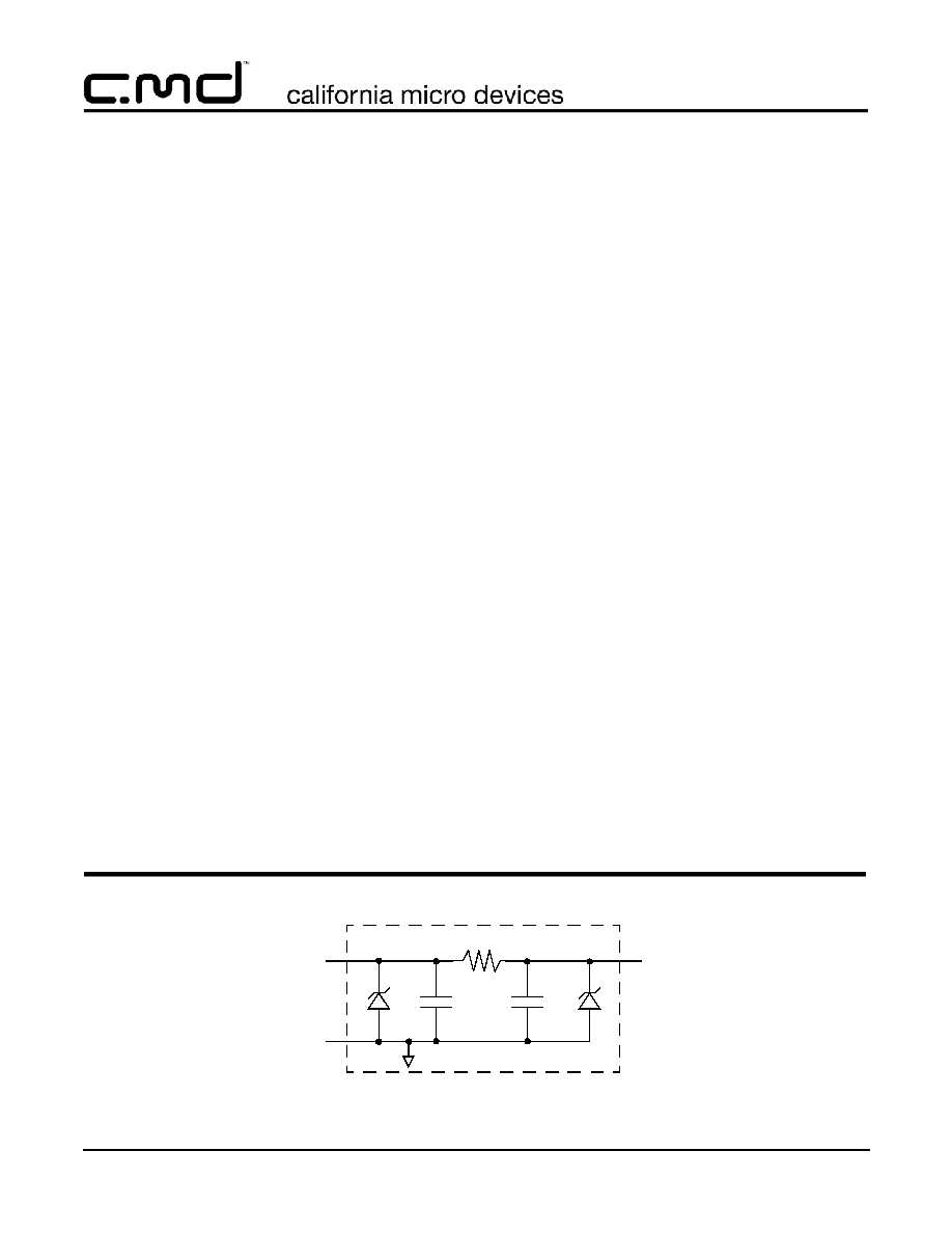
Electrical Schematic
100
30pF
30pF
FILTERn*
GND
FILTERn*
(Pins B1-B3)
1 of 6 EMI/RFI + ESD Channels
* See Package/Pinout Diagram
for expanded pin information.
(Pins A1-A6)
(Pins C1-C6)
© 2005 California Micro Devices Corp. All rights reserved.
2
490 N. McCarthy Blvd., Milpitas, CA 95035-5112
Tel: 408.263.3214
Fax: 408.263.7846
www.cmd.com
11/08/05
CM1440
Ordering Information
Note 1: Parts are shipped in Tape & Reel form unless otherwise specified.
Note 2: Lead-free devices are specified by using a "+" character for the top side orientation mark.
PIN DESCRIPTIONS
PIN(s)
NAME
DESCRIPTION
A1
FILTER1
Filter Channel 1
A2
FILTER2
Filter Channel 2
A3
FILTER3
Filter Channel 3
A4
FILTER4
Filter Channel 4
A5
FILTER5
Filter Channel 5
A6
FILTER6
Filter Channel 6
B1-B3
GND
Device Ground
C1
FILTER1
Filter Channel 1
C2
FILTER2
Filter Channel 2
C3
FILTER3
Filter Channel 3
C4
FILTER4
Filter Channel 4
C5
FILTER5
Filter Channel 5
C6
FILTER6
Filter Channel 6
FILTER5
FILTER6
GND
FILTER5
FILTER6
A6
A5
Orientation
Marking
B3
C6
C5
FILTER3
FILTER4
GND
FILTER3
FILTER4
A4
A3
B2
C4
C3
FILTER1
FILTER2
GND
FILTER1
FILTER2
A2
A1
B1
C2
C1
A1
N406
4
3
2
6
5
1
C
B
A
Orientation
Marking
(see note 2)
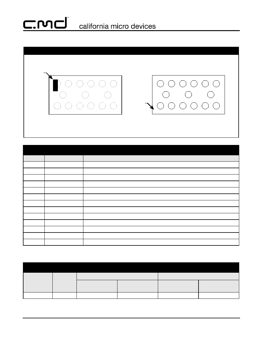
PACKAGE / PINOUT DIAGRAMS
Notes:
BOTTOM VIEW
CM1440-06CS/CP
15 Bump CSP Package
(Bumps Up View)
TOP VIEW
(Bumps Down View)
1) These drawings are not to scale.
2) Lead-free devices are specified by using a "+" character for the top side orientation mark.
PART NUMBERING INFORMATION
Pins
Package
Standard Finish
Lead-free Finish
2
Ordering Part
Number
1
Part Marking
Ordering Part
Number
1
Part Marking
15
CSP
CM1440-06CS
N406
CM1440-06CP
N406
© 2005 California Micro Devices Corp. All rights reserved.
11/08/05
490 N. McCarthy Blvd., Milpitas, CA 95035-5112
Tel: 408.263.3214
Fax: 408.263.7846
www.cmd.com
3
CM1440
Specifications
Note 1: T
A
=25
∞
C unless otherwise specified.
Note 2: ESD applied to input and output pins with respect to GND, one at a time.
Note 3: These parameters are guaranteed by design and characterization.
ABSOLUTE MAXIMUM RATINGS
PARAMETER
RATING
UNITS
Storage Temperature Range
-65 to +150
∞C
DC Power per Resistor
100
mW
DC Package Power Rating
500
mW
STANDARD OPERATING CONDITIONS
PARAMETER
RATING
UNITS
Operating Temperature Range
-40 to +85
∞C
ELECTRICAL OPERATING CHARACTERISTICS
(SEE NOTE1)
SYMBOL
PARAMETER
CONDITIONS
MIN
TYP
MAX
UNITS
R
Resistance
80
100
120
C
TOTAL
Total Channel Capacitance
At 2.5VDC Reverse
Bias, 1MHz, 30mVAC
48
60
72
pF
C
Capacitance C1
At 2.5VDC Reverse
Bias, 1MHz, 30mVAC
24
30
36
pF
V
DIODE
Standoff Voltage
I
DIODE
=10
A
6.0
V
I
LEAK
Diode Leakage Current (reverse bias)
V
DIODE
=
+
3.3V
0.1
1
A
V
SIG
Signal Clamp Voltage
Positive Clamp
Negative Clamp
I
LOAD
= 10mA
5.6
-1.5
6.8
-0.8
9.0
-0.4
V
V
V
ESD
In-system ESD Withstand Voltage
a) Human Body Model, MIL-STD-883, Method
3015
b) Contact Discharge per IEC 61000-4-2 Level 4
Notes 2 and 3
±30
±30
kV
kV
R
DYN
Dynamic Resistance
Positive
Negative
2.3
0.9
f
C
Cut-off Frequency
Z
SOURCE
=50
, Z
LOAD
=50
R=100
, C=30pF
60
MHz
© 2005 California Micro Devices Corp. All rights reserved.
4
490 N. McCarthy Blvd., Milpitas, CA 95035-5112
Tel: 408.263.3214
Fax: 408.263.7846
www.cmd.com
11/08/05
CM1440
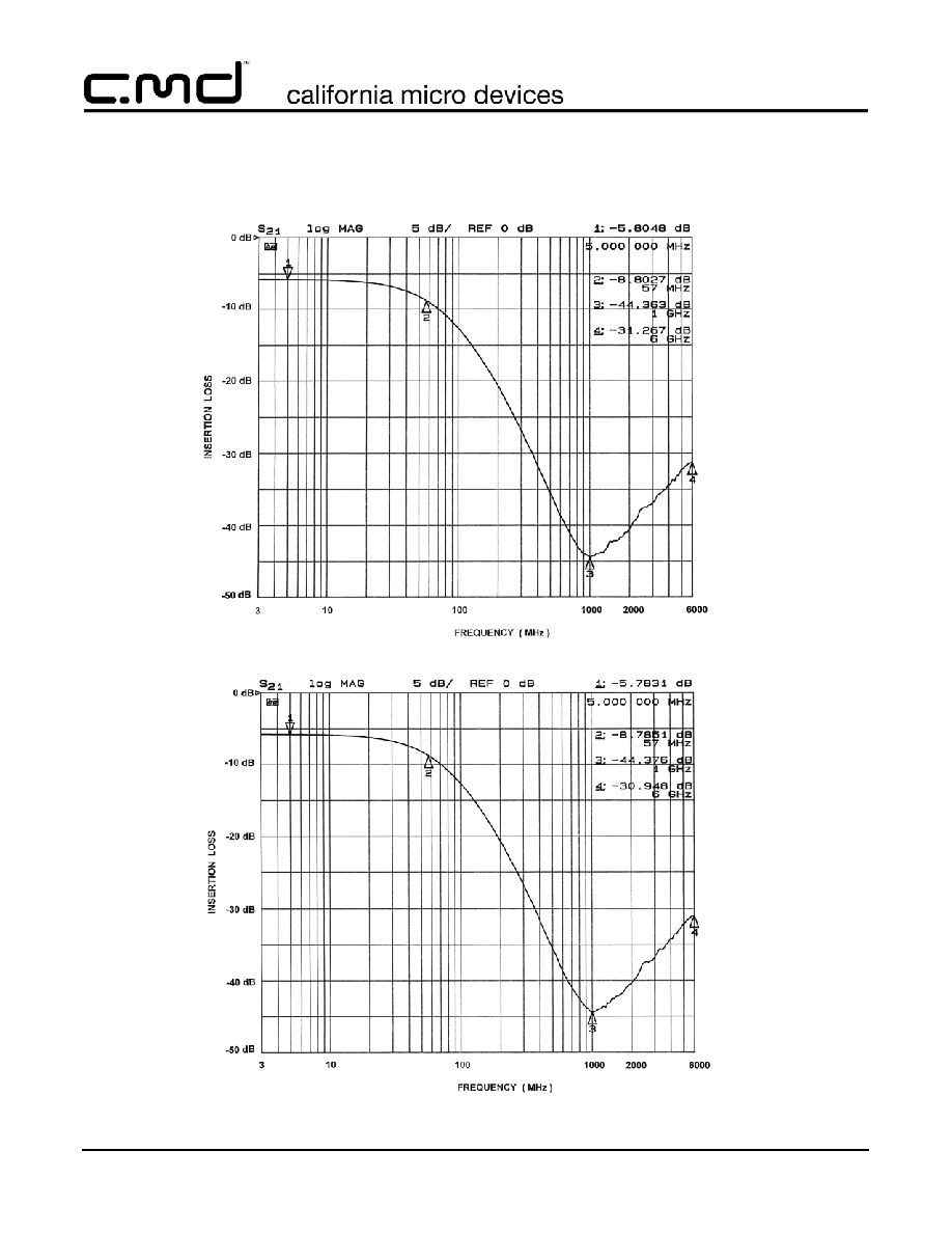
Performance Information
Typical Filter Performance (T
A
=25∞C, DC Bias=0V, 50 Ohm Environment)
Figure 1. Insertion Loss vs. Frequency (A1-C1 to GND B1)
Figure 2. Insertion Loss vs. Frequency (A2-C2 to GND B1)

© 2005 California Micro Devices Corp. All rights reserved.
11/08/05
490 N. McCarthy Blvd., Milpitas, CA 95035-5112
Tel: 408.263.3214
Fax: 408.263.7846
www.cmd.com
5
CM1440
Performance Information (cont'd)
Typical Filter Performance (T
A
=25∞C, DC Bias=0V, 50 Ohm Environment)
Figure 3. Insertion Loss vs. Frequency (A3-C3 to GND B2)
Figure 4. Insertion Loss vs. Frequency (A4-C4 to GND B2)