SI-3002KWF
1 A, Low-Dropout,
Dual Output,
2.5 V & 3.3 V Regulator
115 Northeast Cutoff, Box 15036
Worcester, Massachusetts 01615-0036
Linear
Regulators
2
FUNCTIONAL BLOCK DIAGRAM
Copyright © 2004, 2005 Allegro MicroSystems, Inc.
Recommended Operating Conditions
Min
Max
Units
DC Output Current
0
1
A
Operating Ambient Temp.
-30
+85
°C
Operating Junction Temp.
-20
+100
°C
For the availability of parts meeting -40°C requirements,
contact Allegro's Sales Representative.
Allowable Package Power Dissipation
This data sheet is based on Sanken data sheet SSJ-02006.
SI-3002KWF
1 A, Low-Dropout,
Dual Output,
2.5 V & 3.3 V Regulator
www.allegromicro.com
Linear
Regulators
3
ELECTRICAL CHARACTERISTICS
at T
A
= +25°C, V
E
= 2 V (unless otherwise noted).
Limits
Characteristic
Symbol
Test Conditions
Min.
Typ.
Max.
Units
Channel 1
Output Voltage
V
O1
V
I
= 5.0 V, I
O1
= 10 mA
3.234
3.300 3.366
V
V
O1(off)
V
E
= 0 V
--
--
0.5
V
Output Volt. Temp. Coeff.
a
VO1
0°C
T
J
100°C
--
±0.3
--
mV/°C
Output Short-Circuit Current
I
OM1
V
I
= 5.0 V, See note
1.2
--
--
A
Line Regulation
V
O(
VI)1
V
I
= 4.5 V ~ 10 V, I
O1
= 10 mA
--
--
20
mV
Load Regulation
V
O(
IO)1
V
I
= 5.0 V, I
O1
= 0 A ~ 1.0 A
--
--
30
mV
Dropout Voltage
V
Imin
- V
O1
I
O1
= 1.0 A
--
--
0.6
V
Ripple Rejection Ratio
PSRR
V
I
= 5.0 V, 100 Hz
f
120 Hz
--
60
--
dB
Channel 2
Output Voltage
V
O2
V
I
= 5.0 V, I
O2
= 10 mA
2.450
2.500 2.550
V
V
O2(off)
V
E
= 0 V
--
--
0.5
V
Output Volt. Temp. Coeff.
a
VO2
0°C
T
J
100°C
--
±0.3
--
mV/°C
Output Short-Circuit Current
I
OM2
V
I
= 5.0 V, See note
1.2
--
--
A
Line Regulation
V
O(
VI)2
V
I
= 4.5 V ~ 10 V, I
O2
= 10 mA
--
--
20
mV
Load Regulation
V
O(
IO)2
V
I
= 5.0 V, I
O2
= 0 A ~ 1.0 A
--
--
30
mV
Dropout Voltage
V
Imin
- V
O2
I
O2
= 1.0 A
--
--
0.6
V
Ripple Rejection Ratio
PSRR
V
I
= 5.0 V, 100 Hz
f
120 Hz
--
60
--
dB
Logic
Ground Terminal Current
I
GND
V
I
= 5.0 V, I
O
= 0 mA, V
E
= 2.0 V
--
1.0
1.5
mA
V
I
= 5.0 V, V
E
= 0 V
--
--
0.5
mA
Enable Input Voltage
V
EH
Output ON
2.0
--
--
V
V
EL
Output OFF
--
--
0.8
V
Enable Input Current
I
EH
V
E
= 2.7 V
--
0
5.0
µA
I
EL
V
E
= 0.4 V
--
-12
-100
µA
Thermal Shutdown
T
J
I
O
= 10 mA
135
150
--
°C
Typical values are given for circuit design information only.
Note: Output short-circuit current is at point where output voltage has decreased 5%.
SI-3002KWF
1 A, Low-Dropout,
Dual Output,
2.5 V & 3.3 V Regulator
115 Northeast Cutoff, Box 15036
Worcester, Massachusetts 01615-0036
Linear
Regulators
4
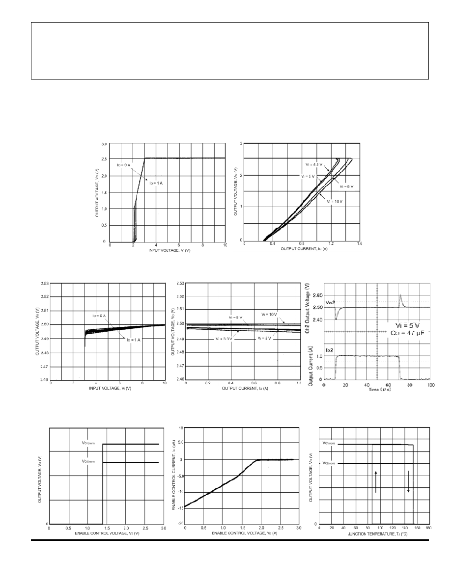
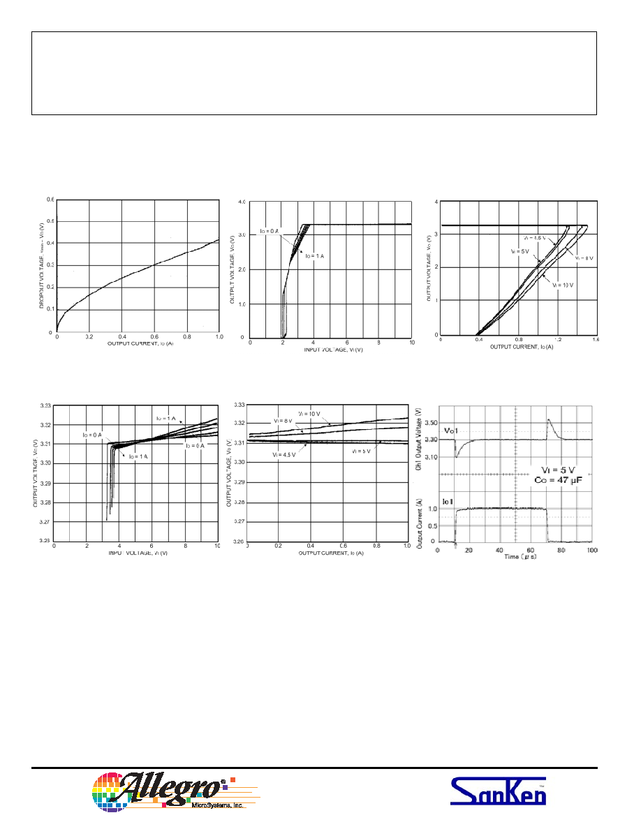
TYPICAL CHARACTERISTICS
(V
I
= 5.0 V, T
A
= 25°C)
Chan. 1 Dropout Voltage
Chan. 1 Low-Voltage Behavior
Chan. 1 Overcurrent Protection
Chan. 1 Line Regulation
Chan. 1 Load Regulation
Chan. 1 Transient Response

SI-3002KWF
1 A, Low-Dropout,
Dual Output,
2.5 V & 3.3 V Regulator
115 Northeast Cutoff, Box 15036
Worcester, Massachusetts 01615-0036
Linear
Regulators
6
Input Capacitor
(C
I
,
0.1 10
µF). This is necessary
either when the input line includes inductance or when the
wiring is long.
Output Capacitor
(C
O
,
>
22 µF). This device is not
designed for a use with a very low ESR output capacitor
such as a ceramic capacitor. Output oscillation may occur
with that kind of capacitor.
ENABLE Input
. The ENABLE (control) input features
an internal pull-up resistor. Leaving this input open causes
the output to turn on.
Parallel Operation.
Parallel operation to increase load
current is not permitted.
Determination of DC Input Voltage.
The minimum
input voltage V
I
(min) should be higher than the sum of the
fixed output voltage and the maximum rated dropout
voltage.
Overcurrent Protection.
The SI-3000KWF series has
a built-in fold-back type overcurrent protection circuit,
which limits the output current at a start-up mode. It thus
cannot be used in applications that require current at the
start-up mode such as:
(1) constant-current load,
(2) power supply with positive and negative outputs to
common load (a center-tap type power supply), or
(3) raising the output voltage by putting a diode or a
resistor between the device ground and system ground.
Thermal Protection.
Circuitry turns off the pass
transistor when the junction temperature rises above 135°C.
It is intended only to protect the device from failures due to
excessive junction temperatures and should not imply that
output short circuits or continuous overloads are permitted.
APPLICATIONS INFORMATION
Heat Radiation and Reliability.
The reliability of the
IC is directly related to the junction temperature (T
J
) in its
operation. Accordingly, careful consideration should be
given to heat dissipation.
The inner frame on which the integrated circuit is mounted
is connected to the GND terminal (pin 3). Therefore, it is
very effective for heat radiation to enlarge the copper area
that is connected to the GND terminal. The graph on page
2 illustrates the effect of thermal resistance on the allow-
able package power dissipation.
The junction temperature (T
J
) can be determined from
either of the following equations:
T
J
= (P
D
× R
JA
) + T
A
or
T
J
= (P
D
× R
JC
) + T
C
where P
D
= I
O1
(V
I
V
O1
) + I
O2
(V
I
V
O2
) and
R
JC
= 7°C/W.