Designed to meet the high-current requirements in industrial and
consumer applications; embedded core, memory, or logic supplies; TVs,
VCRs, and office equipment, the SI-3003KWD voltage regulator offers
the reduced dropout voltage and low quiescent current essential for
improved efficiency. This device delivers dual regulated outputs at up to
1 A. Integrated thermal and overcurrent protection enhance overall
system reliability. Devices with other output voltages are also available.
Quiescent current does not increase significantly as the dropout
voltage is approached, an ideal feature in standby/resume power systems
where data integrity is crucial. Regulator accuracy and excellent
temperature characteristics are provided by a bandgap reference. An
LS-TTL/CMOS-compatible input gives the designer complete control
over power up, standby, or power down. A pnp pass element provides a
dropout voltage of less than 600 mV at 1 A of load current. Low output
voltages eliminate the need for expensive PWM buck converters. The
low dropout voltage permits more efficient regulation before output
regulation is lost.
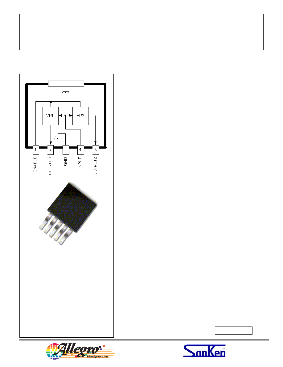
This device is supplied in a 5-lead surface-mount plastic package
(TO-263) with ground tab to provide a low-resistance path for maximum
heat dissipation. A similar device in a flange-mounted (TO-220-style)
high-power package is the SI-3003KWF.
FEATURES
1 A Output Current per Channel
0.6 V Maximum Dropout Voltage at I
O
= 1 A
Fast Transient Response
1.5 mA Maximum Standby Current
Foldback Current Limiting
Ground Tab for Superior Heat Dissipation
Thermal Protection
APPLICATIONS
TVs, VCRs, Electronic Games
Embedded Core, Memory, or Logic Supplies
Printers and Other Office Equipment
Industrial Machinery
Secondary-Side Stabilization of Multi-Output SMPS
1 A, Low-Dropout, Dual Output, 1.8 V & 2.5 V Regulator
Data Sheet
27468.311*
Always order by complete part number, e.g., SI-3003KWD-TL ,
where "-TL" indicates tape and reel.
ABSOLUTE MAXIMUM RATINGS
Input Voltage, V
I
. . . . . . . . . . . . . 18 V
Output Current, I
O
. . . . . . . . . . . . . 1 A*
Enable Input Voltage, V
E
. . . . . . . 6.0 V
Junction Temperature, T
J
. . . . +125°C
Storage Temperature Range,
T
S
. . . . . . . . . . . . -40°C to +125°C
* Output current rating is limited by input
voltage, duty cycle, and ambient tempera-
ture. Under any set of conditions, do not
exceed a junction temperature of +125°C.
SI-3003KWD
Sanken Power Devices
from Allegro MicroSystems
Linear
Regulators
SI-3003KWD
1 A, Low-Dropout,
Dual Output,
1.8 V & 2.5 V Regulator
115 Northeast Cutoff, Box 15036
Worcester, Massachusetts 01615-0036
Linear
Regulators
2
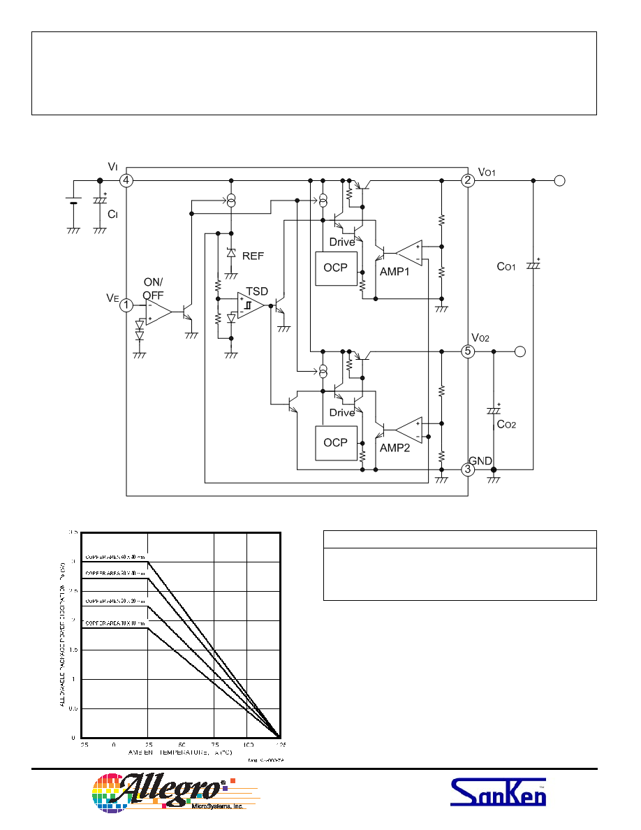
FUNCTIONAL BLOCK DIAGRAM
Copyright © 2004, 2005 Allegro MicroSystems, Inc.
Recommended Operating Conditions
Min
Max
Units
DC Output Current
0
1
A
Operating Ambient Temp.
-30
+85
°C
Operating Junction Temp.
-20
+100
°C
For the availability of parts meeting -40°C requirements,
contact Allegro's Sales Representative.
Allowable Package Power Dissipation
This data sheet is based on Sanken data sheet SSJ-02009A.
SI-3003KWD
1 A, Low-Dropout,
Dual Output,
1.8 V & 2.5 V Regulator
www.allegromicro.com
Linear
Regulators
3
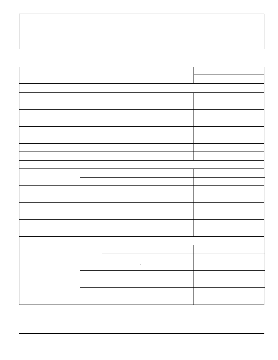
ELECTRICAL CHARACTERISTICS
at T
A
= +25°C, V
E
= 2 V (unless otherwise noted).
Limits
Characteristic
Symbol
Test Conditions
Min.
Typ.
Max.
Units
Channel 1
Output Voltage
V
O1
V
I
= 3.3 V, I
O1
= 10 mA
2.450
2.500 2.550
V
V
O1(off)
V
E
= 0 V
--
--
0.5
V
Output Volt. Temp. Coeff.
a
VO1
0°C
T
J
100°C
--
±0.3
--
mV/°C
Output Short-Circuit Current
I
OM1
V
I
= 3.3 V, See note
1.2
--
--
A
Line Regulation
V
O(
VI)1
V
I
= 3.2 V ~ 5.0 V, I
O1
= 10 mA
--
--
20
mV
Load Regulation
V
O(
IO)1
V
I
= 3.3 V, I
O1
= 0 A ~ 1.0 A
--
--
30
mV
Dropout Voltage
V
Imin
- V
O1
I
O1
= 1.0 A
--
--
0.6
V
Ripple Rejection Ratio
PSRR
V
I
= 3.3 V, 100 Hz
f
120 Hz
--
60
--
dB
Channel 2
Output Voltage
V
O2
V
I
= 3.3 V, I
O2
= 10 mA
1.764
1.800 1.836
V
V
O2(off)
V
E
= 0 V
--
--
0.5
V
Output Volt. Temp. Coeff.
a
VO2
0°C
T
J
100°C
--
±0.3
--
mV/°C
Output Short-Circuit Current
I
OM2
V
I
= 3.3 V, See note
1.2
--
--
A
Line Regulation
V
O(
VI)2
V
I
= 3.2 V ~ 5.0 V, I
O2
= 10 mA
--
--
20
mV
Load Regulation
V
O(
IO)2
V
I
= 3.3 V, I
O2
= 0 A ~ 1.0 A
--
--
30
mV
Dropout Voltage
V
Imin
- V
O2
I
O2
= 1.0 A
--
--
0.6
V
Ripple Rejection Ratio
PSRR
V
I
= 3.3 V, 100 Hz
f
120 Hz
--
60
--
dB
Logic
Ground Terminal Current
I
GND
V
I
= 3.3 V, I
O
= 0 mA, V
E
= 2.0 V
--
1.0
1.5
mA
V
I
= 3.3 V, V
E
= 0 V
--
--
0.5
mA
Enable Input Voltage
V
EH
Output ON
2.0
--
--
V
V
EL
Output OFF
--
--
0.8
V
Enable Input Current
I
EH
V
E
= 2.7 V
--
0
5.0
µA
I
EL
V
E
= 0.4 V
--
-12
-100
µA
Thermal Shutdown
T
J
I
O
= 10 mA
135
150
--
°C
Typical values are given for circuit design information only.
Note: Output short-circuit current is at point where output voltage has decreased 5%.
SI-3003KWD
1 A, Low-Dropout,
Dual Output,
1.8 V & 2.5 V Regulator
115 Northeast Cutoff, Box 15036
Worcester, Massachusetts 01615-0036
Linear
Regulators
4
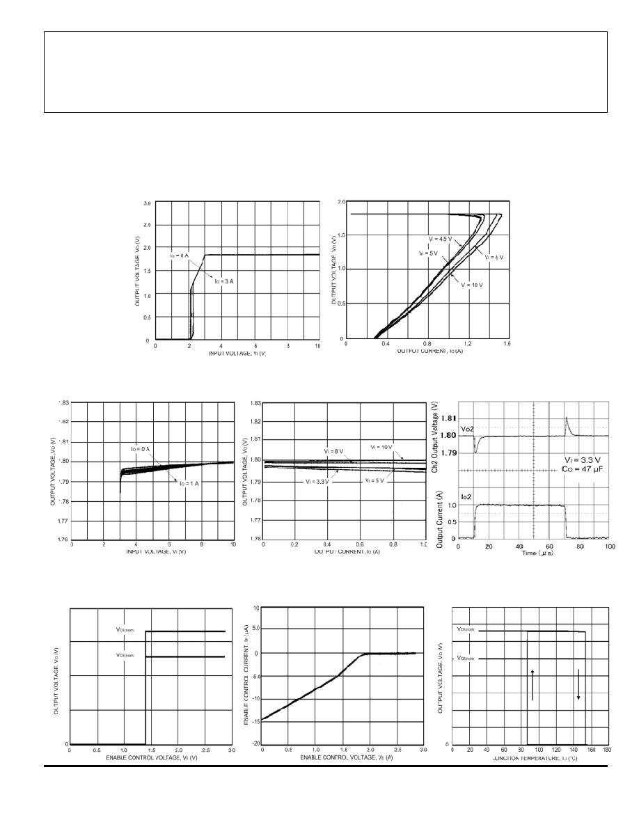
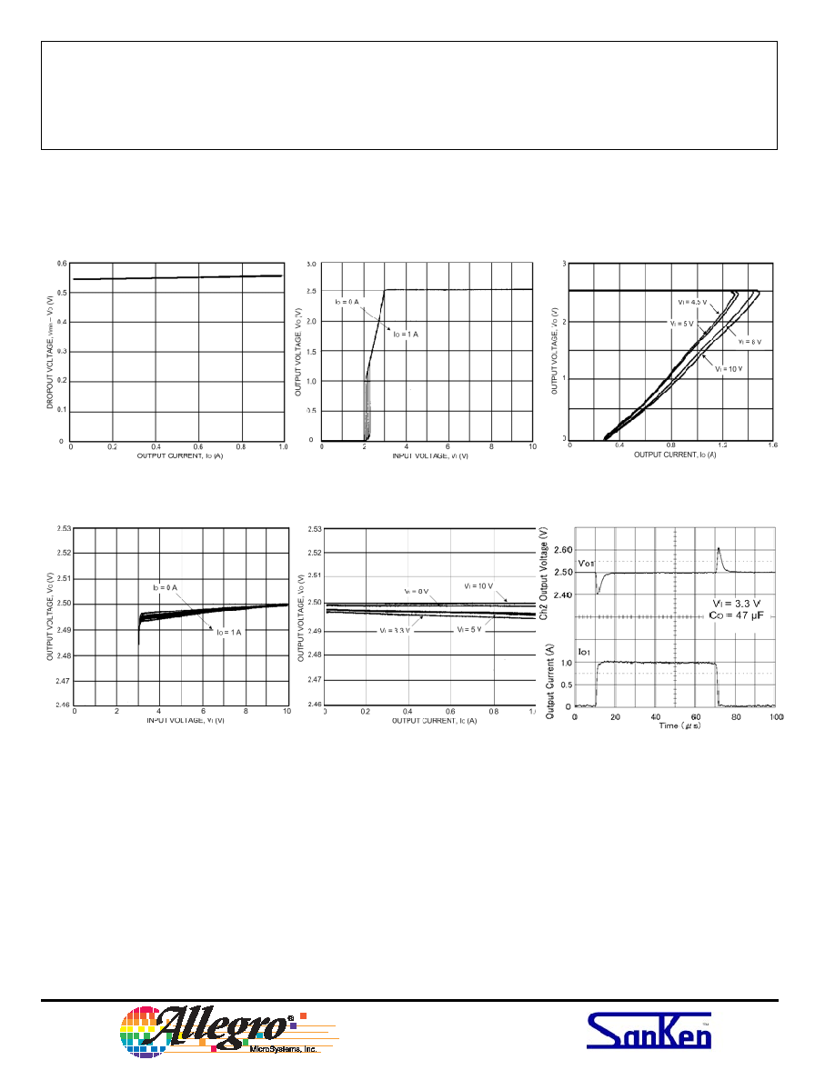
TYPICAL CHARACTERISTICS
(V
I
= 3.3 V, T
A
= 25°C)
Chan. 1 Dropout Voltage
Chan. 1 Low-Voltage Behavior
Chan. 1 Overcurrent Protection
Chan. 1 Line Regulation
Chan. 1 Load Regulation
Chan. 1 Transient Response