Data Sheet
27468.25
LOW-VOLTAGE, HIGH-CURRENT
2.5 V LINEAR REGULATOR
The SI-3025LSA is designed to meet the requirement for increased
integration and reliability in low-voltage, high-current, linear regulator
applications such as personal computers (PCs) and set-top boxes. Each
device incorporates a monolithic low-level reference and control circuit
with a high-current pnp transistor in a power multi-chip module
(PMCMTM). Regulated output voltages of 1.8 V or 3.3 V are also
available.
The high-current pass element provides a low dropout voltage with
output current to 1 A. Regulator accuracy of
±
2 % and excellent
temperature characteristics are provided. The logic-compatible
ENABLE input gives the designer complete control over power up,
power down, and standby or sleep.
These devices are supplied in a fully molded 8-lead miniature
surface-mount package (tape and reel) with enhanced power-dissipating
qualities. They are rated for continuous operation between -30
°
C and
+100
°
C.
FEATURES
s
1 A Output Current
s
Low Dropout voltage
s
LSTTL/CMOS-Compatible On/Off Control
Less Than 1
µ
A "Sleep" Current
s
Internal Foldback Overcurrent Limiting
s
Internal Thermal Shutdown
s
Surface-Mount Package
Always order by complete part number: SI-3025LSA-TL ,
where "-TL" indicates tape and reel.
ABSOLUTE MAXIMUM RATINGS
Input Voltage, V
I
................................ 16 V
Supply Voltage, V
S
............................ 16 V
Continuous Output Current, I
O
........ 1.0 A*
Logic Input Voltage, V
E
......................... V
S
Package Power Dissipation,
P
D
........................................ See Graph
Output Junction Temperature,
T
J
............................................ +150
°
C
Operating Temperature Range,
T
A
............................... -30
°
C to +100
°
C
Storage Temperature Range,
T
stg
............................. -30
°
C to +150
°
C
* Output current rating may be limited by duty
cycle, ambient temperature, and heat sinking.
Under any set of conditions, do not exceed the
specified current rating or a junction temperature
of 150°C.
Fault conditions that produce excessive
junction temperature will activate the device's
thermal shutdown circuitry. These conditions
can be tolerated but should be avoided.
SI-3025LSA
1
2
3
4
5
6
7
8
Dwg. PK-012
IN
GND
OUT
INTERNAL
CONNECTION
ENABLE
SUPPLY
GND
OUT
IC
VR
SUB
V
S
TM
115 Northeast Cutoff, Box 15036
Worcester, Massachusetts 01615-0036 (508) 853-5000
SI-3025LSA
LOW-VOLTAGE, HIGH-CURRENT
2.5 V LINEAR REGULATOR
TM
2
FUNCTIONAL BLOCK DIAGRAM
Copyright © 2001 Allegro MicroSystems, Inc.
1.5
1.0
0.5
20
60
100
40
0
AMBIENT TEMPERATURE in
°
°
°
°
C
ALLOWABLE PACKAGE POWER DISSIPATION in WATTS
Dwg. GK-010-1
80
120
0
56.5 mm x 56.5 mm
COPPER AREA ON
GLASS-EPOXY BOARD
140
28 mm x 28 mm
COPPER AREA ON
GLASS-EPOXY BOARD
40 mm x 40 mm
COPPER AREA ON
GLASS-EPOXY BOARD
20 mm x 20 mm
COPPER AREA ON
GLASS-EPOXY BOARD
Leads 7 and 8 are soldered to
the copper area and provide
heat sinking of the pass transis-
tor.
RECOMMENDED OPERATING CONDITIONS
Max. Input Voltage, V
I
................................................ 3.5 V
Output Current, I
O
.......................................... 0 A to 1.0 A
Output Junction Temperature Range, T
J
-20
°
C to +125
°
C
Ambient Temperature Range, T
A
.............. -30
°
C to +85
°
C
INPUT
1
SUPPLY
3
OUTPUT
OUTPUT
8
7
6
Dwg. FK-019
GROUND
GROUND
5
4
2
ENABLE
INTERNAL
CONNECTION
SUB
+
THERMAL
PROTECTION
115 Northeast Cutoff, Box 15036
Worcester, Massachusetts 01615-0036 (508) 853-5000
SI-3025LSA
LOW-VOLTAGE, HIGH-CURRENT
2.5 V LINEAR REGULATOR
TM
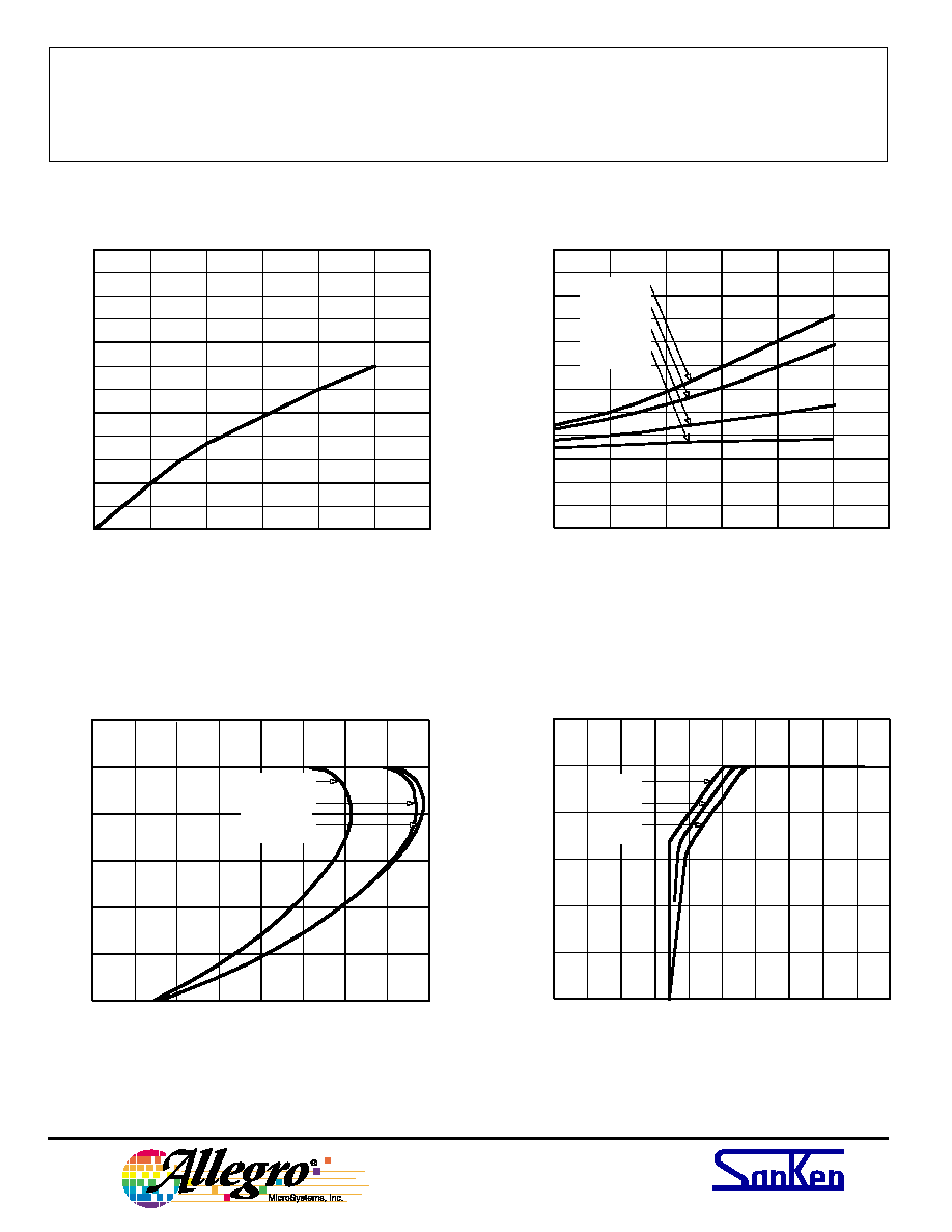
4
TYPICAL CHARACTERISTICS at T
A
= 25
°
C
0.2
0.1
0
0.3
0.4
0.5
0.4
0.8
OUTPUT CURRENT in AMPERES
0
Dwg. GK-025-1
DROPOUT VOLTAGE
1.2
0.6
1.0
0.2
0.6
2.50
2.48
2.46
2.52
2.54
2.56
0.4
0.8
OUTPUT CURRENT in AMPERES
0
Dwg. GK-026-1
OUTPUT VOLTAGE
1.2
0.6
1.0
0.2
2.58
V
I
= V
S
= 10 V
V
I
= V
S
= 8 V
V
I
= V
S
= 5 V
V
I
= V
S
= 3.2 V
0
1.0
2.0
OUTPUT CURRENT in AMPERES
0
Dwg. GK-027-1
OUTPUT VOLTAGE
2.0
1.0
1.5
0.5
3.0
V
I
= V
S
= 3.2 V
V
I
= V
S
= 5 V
V
I
= V
S
= 6 V
INPUT VOLTAGE
0
Dwg. GK-028-1
OUTPUT VOLTAGE
5.0
3.0
4.0
1.0
2.0
I
O
= 0 A
I
O
= 0.5 A
I
O
= 1 A
0
1.0
2.0
3.0
Dropout voltage
Load regulation
Overcurrent protection
V
OUT
vs V
IN