 | –≠–ª–µ–∫—Ç—Ä–æ–Ω–Ω—ã–π –∫–æ–º–ø–æ–Ω–µ–Ω—Ç: SI-8050JD | –°–∫–∞—á–∞—Ç—å:  PDF PDF  ZIP ZIP |
Designed to meet high-current requirements at high efficiency in
industrial and consumer applications; embedded core, memory, or logic
supplies; TVs, VCRs, and office or telecommunications equipment, the
SI-8050JD dc/dc step-down (buck) converter offers a constant 125 kHz
switching frequency essential for low EMI noise. The npn switch is
included on the die along with the oscillator, control, and logic circuitry
requiring only four external components for a regulated 5.0 V output at
up to 1.5 A. .
A wide input voltage range and integrated thermal and overcurrent
protection enhance overall system reliability. Reference accuracy and
excellent temperature characteristics are provided. An output-enable
input gives the designer complete control over power up, standby, or
power down.
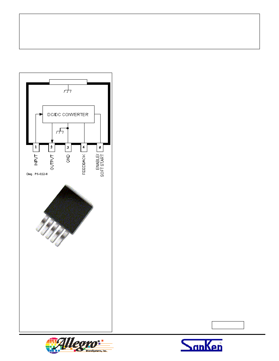
This device is supplied in a 5-lead surface-mount plastic package
(TO-263) with ground tab to provide a low-resistance path for maximum
heat dissipation. A similar device in a flange-mounted (TO-220-style)
high-power package is the SI-8050JF.
FEATURES
7 V to 40 V Input Range
1.5 A Output Current at 5.0 V
2% Output Voltage Tolerance
Foldback Current Limiting
Constant 125 kHz Switching Frequency
200 µA Maximum Standby Current
Soft Start Prevents Supply Voltage Dip
Remote Voltage Sensing
Exposed Pad for Superior Heat Dissipation
Thermal Protection
APPLICATIONS
TVs, VCRs, Electronic Games
Embedded Core, Memory, or Logic Supplies
Printers and Other Office Equipment
Industrial Machinery
Telecommunications Equipment
Step-Down to 5.0 V, 1.5 A, DC/DC Converter
Data Sheet
27469.31*
Always order by complete part number, e.g., SI-8050JD-TL ,
where "-TL" indicates tape and reel.
ABSOLUTE MAXIMUM RATINGS
Input Voltage, V
I
. . . . . . . . . . . . . 43 V
Output Current, I
O
. . . . . . . . . . . 1.5 A*
Enable Input Voltage, V
OE
. . . . . . . . . . .
6 V
Junction Temperature, T
J
. . . . +125∞C
Storage Temperature Range,
T
S
. . . . . . . . . . . . -40∞C to +125∞C
* Output current rating is limited by input
voltage, duty cycle, and ambient tempera-
ture. Under any set of conditions, do not
exceed a junction temperature of +125∞C.
SI-8050JD
Sanken Power Devices
from Allegro MicroSystems
Switching
Regulators
SI-8050JD
Step-Down
to 5.0 V, 1.5 A,
DC/DC Converter
115 Northeast Cutoff, Box 15036
Worcester, Massachusetts 01615-0036
Switching
Regulators
2
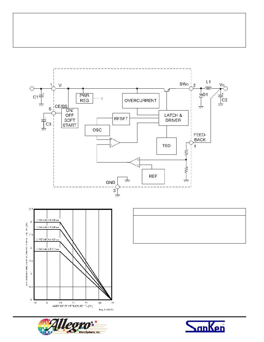
FUNCTIONAL BLOCK DIAGRAM
Copyright © 2004, 2005 Allegro MicroSystems, Inc.
Recommended Operating Conditions
Min
Max
Units
DC Input Voltage (I
O
1 A)
7
8
V
(I
O
1.5 A)
8
40
V
DC Output Current (V
I
6.3 V)
0
1.5
A
Operating Junction Temp.
-30
+125
∞C
For the availability of parts meeting -40∞C require-
ments, contact Allegro's Sales Representative.
Allowable Package Power Dissipation
This data sheet is based on Sanken data sheet SSJ-02486
SI-8050JD
Step-Down
to 5.0 V, 1.5 A,
DC/DC Converter
www.allegromicro.com
Switching
Regulators
3
ELECTRICAL CHARACTERISTICS
at T
A
= +25∞C, V
I
= 20 V, I
O
= 0.5 A (unless otherwise noted).
Limits
Characteristic
Symbol
Test Conditions
Min.
Typ.
Max.
Units
Output Voltage
V
O
4.90
5.00
5.10
V
Ref. Volt. Temp. Coeff.
a
Vref
--
±0.5
--
mV/∞C
Output Short-Circuit Current
I
OM
See note
1.6
--
--
A
Efficiency
--
82
--
%
Operating Frequency
f
--
125
--
kHz
Line Regulation
V
O(
VI)
V
I
= 10 V ~ 30 V, I
O
= 0.5 A
--
40
100
mV
Load Regulation
V
O(
IO)
V
I
= 20 V, I
O
= 0.2 A ~ 0.8 A
--
10
40
mV
Quiescent Current
I
IQ
I
O
= 0 A
--
7.0
--
mA
V
CE
= 0.3 V
--
--
200
µA
Chip Enable Voltage
V
CE
Converter turn-off voltage
--
--
0.5
V
Soft-Start Current
I
SS
V
SS
= 0 V
--
--
-100
µA
Typical values are given for circuit design information only.
Note: Output short-circuit current is at point where output voltage has decreased 5% below V
O(nom)
.
SI-8050JD
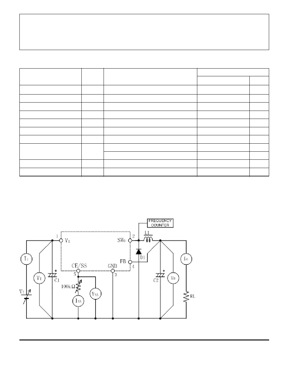
Test Circuit
C1 = 220 µF/50 V
C2 = 470 µF/25 V
C3 = 0.47 µF/10 V
L1 = 100 µH
D1 = Sanken SFPB-66
SI-8050JD
Step-Down
to 5.0 V, 1.5 A,
DC/DC Converter
115 Northeast Cutoff, Box 15036
Worcester, Massachusetts 01615-0036
Switching
Regulators
4
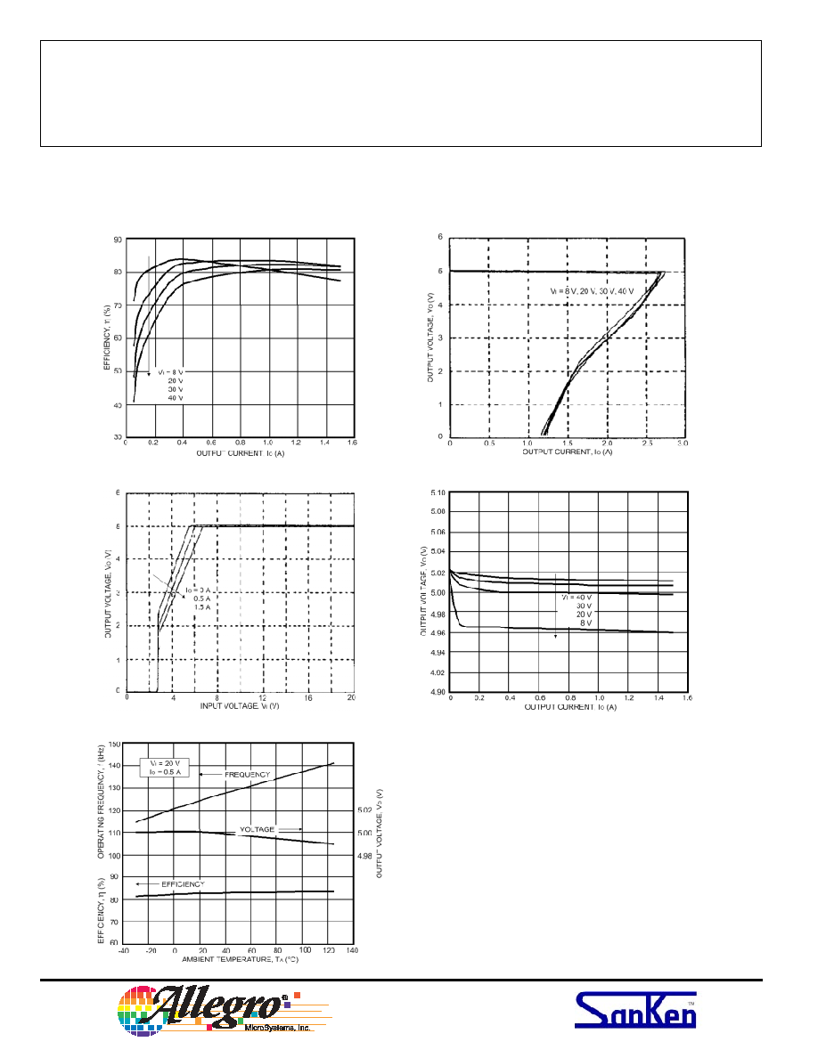
TYPICAL CHARACTERISTICS
(T
A
= 25∞C)
Efficiency
Overcurrent Protection
Low-Voltage Behavior
Load Regulation
Temperature Stability
SI-8050JD
Step-Down
to 5.0 V, 1.5 A,
DC/DC Converter
www.allegromicro.com
Switching
Regulators
5
APPLICATIONS INFORMATION
Input Capacitor
(C1). Capacitors with low impedance
for high-frequency ripple current must be used.
Output Capacitor
(C2). Capacitors with low impedance
for high-frequency ripple current must be used. Especially
when the C2 impedance is high, the switching waveform
may not be normal at low temperatures. Film or tantalum
capacitor for C2 may cause abnormal oscillations.
Catch Diode
(D1). Diode D1 must be a Schottky diode.
Other diode types will result in increased forward voltage
spikes, reverse current flow, increased IC power dissipa-
tion during the off period, and possible destruction of the
IC.
Choke Coil (L1)
. If the winding resistance of the choke
coil is too high, the circuit efficiency will decrease. As the
overcurrent protection start current is approximately 2.5 A,
attention must be paid to the heating of the coil by magnetic
saturation due to overload. To reduce the output ripple, the
inductor may be increased at the expense of excessive
board area and cost.
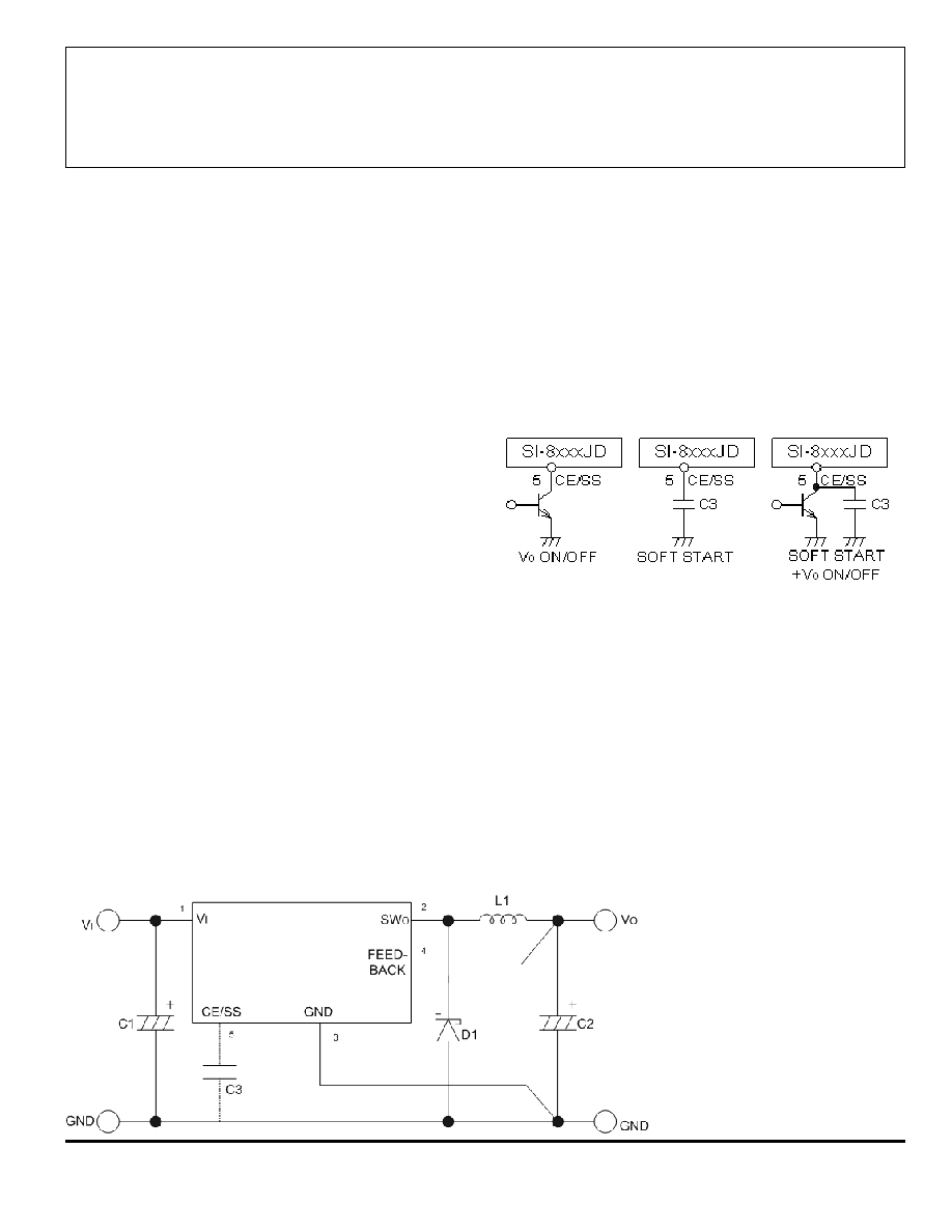
Typical Application
SI-8050JD
Soft-Start Capacitor (C3).
Soft start for the converter
is enabled by connecting a capacitor between terminal 5
and ground. The converter may be turned off by decreasing
the terminal 5 voltage below 0.5 V with either an npn
small-signal transistor or the output of open-collector TTL.
If both a large soft-start capacitor and on/off control are
desired, collector current limiting must be used to prevent
transistor damage. No external voltage can be applied to
terminal 5.
Parallel Operation.
Parallel operation to increase load
current is not permitted.
Overcurrent Protection.
The SI-8000JD series has a
built-in fold-back type overcurrent protection circuit, which
limits the output current at a start-up mode. It thus cannot
be used in applications that require current at the start-up
mode such as:
(1) constant-current load,
(2) power supply with positive and negative outputs to
common load (a center-tap type power supply), or
(3) raising the output voltage by putting a diode or a
resistor between the device ground and system ground.