 | –≠–ª–µ–∫—Ç—Ä–æ–Ω–Ω—ã–π –∫–æ–º–ø–æ–Ω–µ–Ω—Ç: SLA7042M | –°–∫–∞—á–∞—Ç—å:  PDF PDF  ZIP ZIP |
The SLA7042M and SLA7044M are designed for high-efficiency
and high-performance microstepping operation of 2-phase, unipolar
stepper motors. Microstepping provides improved resolution without
limiting step rates, and provides much smoother low-speed motor
operation. An automated, innovative packaging technology combined
with power NMOS FETs and monolithic CMOS logic/control circuitry
advances power multi-chip modules (PMCMsTM) toward the complete
integration of motion control. Each half of these stepper motor control-
ler/drivers operate independently. The 4-bit shift registers are serially
loaded with motor phase information and output current-ratio data (eight
levels). The combination of user-selectable current-sensing resistor,
linearly adjustable reference voltage, and digitally selected output
current ratio provides users with a broad, variable range of of full, half,
and microstepping motor control (I
OUT
[V
REF
/3 ∑ R
S
] ∑ Current Ratio).
Each PMCM is rated for a maximum motor supply voltage of 46 V
and utilizes advanced NMOS FETs for the high-current, high-voltage
driver outputs. The avalanche-rated (
100 V) FETs provide excellent
ON resistance, improved body diodes, and very-fast switching. The
multi-chip ratings and performance afford significant benefits and
advantages for stepper drives when compared to the higher dissipation
and slower switching speeds associated with bipolar transistors. Highly
automated manufacturing techniques provide low-cost and exception-
ally reliable PMCMs suitable for controlling and directly driving a broad
range of 2-phase, unipolar stepper motors. The SLA7042M and
SLA7044M are identical except for r
DS(on)
and output current ratings.
Complete applications information is given on the following pages.
PWM current is regulated by appropriately choosing current-sensing
resistors, a voltage reference, and digitally programmable current ratio.
Inputs are compatible with 5 V logic and microprocessors.
BENEFITS AND FEATURES
s
Cost-Effective, Multi-Chip Solution
s
`Turn-Key' Motion-Control Module
s
Motor Operation to 3 A and 46 V
s
3
rd
Generation High-Voltage FETs
s
100 V, Avalanche-Rated NMOS
s
Low r
DS(on)
NMOS Outputs
s
Advanced, Improved Body Diodes
s
Microstepping Unipolar Drive
s
High-Efficiency, High-Speed PWM
MICROSTEPPING, UNIPOLAR PWM,
HIGH-CURRENT MOTOR CONTROLLER/DRIVER
Always order by complete part number: SLA7042M .
Data Sheet
28202A*
REF/ENABLE A
V
REF
V
CC
1
2
3
4
5
6
7
8
9
10
11
12
13
14
15
16
17
18
Dwg. PK-008
OUT A
OUT B
SENSEA
GROUND A
CNTRL SPLY A
V
REF
V
CC
OUTA
CONTROL/LOGIC
OUT B
GROUND B
REF/ENABLE B
CNTRL SPLY B
SERIAL DATA A
CLOCK A
SERIAL DATA B
CLOCK B
SENSE B
STROBEA
STROBE B
SR/LATCH
¯
+
D/A
CONTROL/LOGIC
¯
SR/LATCH
D/A
+
ABSOLUTE MAXIMUM RATINGS
at T
A
= +25
∞
C
Load Supply Voltage, V
BB
. . . . . . . . . . . . 46 V
FET Output Voltage, V
DS
. . . . . . . . . . . 100 V
Control Supply Voltage, V
DD
. . . . . . . . . 7.0 V
Peak Output Current,
I
OUTM
(t
w
10
µ
s) . . . . . . . . . . . . . . . . 5.0 A
Continuous Output Current, I
OUT
SLA7042M . . . . . . . . . . . . . . . . . . . . . 1.5 A
SLA7044M . . . . . . . . . . . . . . . . . . . . . 3.0 A
Input Voltage Range,
V
IN
. . . . . . . . . . . . . . -0.3 V to V
DD
+ 0.3 V
Reference Voltage, V
REF
. . . . . . . . . . . . V
DD
Package Power Dissipation, P
D
. See Graph
Junction Temperature, T
J
. . . . . . . . . +150
∞
C
Operating Temperature Range,
T
A
. . . . . . . . . . . . . . . . . . . . -20
∞
C to +85
∞
C
Storage Temperature Range,
T
stg
. . . . . . . . . . . . . . . . . . -40
∞
C to +150
∞
C
s
Independent PWM Current Control
(2-Phase)
s
Digitally Programmable PWM
Current Control
s
Low Component-Count PWM Drive
s
Low Internal-Power Dissipation
s
Electrically Isolated Power Tab
s
Logic IC- and
µ
P-Compatible
Inputs
s
Machine-Insertable Package
SLA7042M
AND
SLA7044M
TM
SLA7042M
AND
SLA7044M
MICROSTEPPING,
UNIPOLAR PWM, HIGH-CURRENT
MOTOR CONTROLLER/DRIVERS
115 Northeast Cutoff, Box 15036
Worcester, Massachusetts 01615-0036 (508) 853-5000
TM
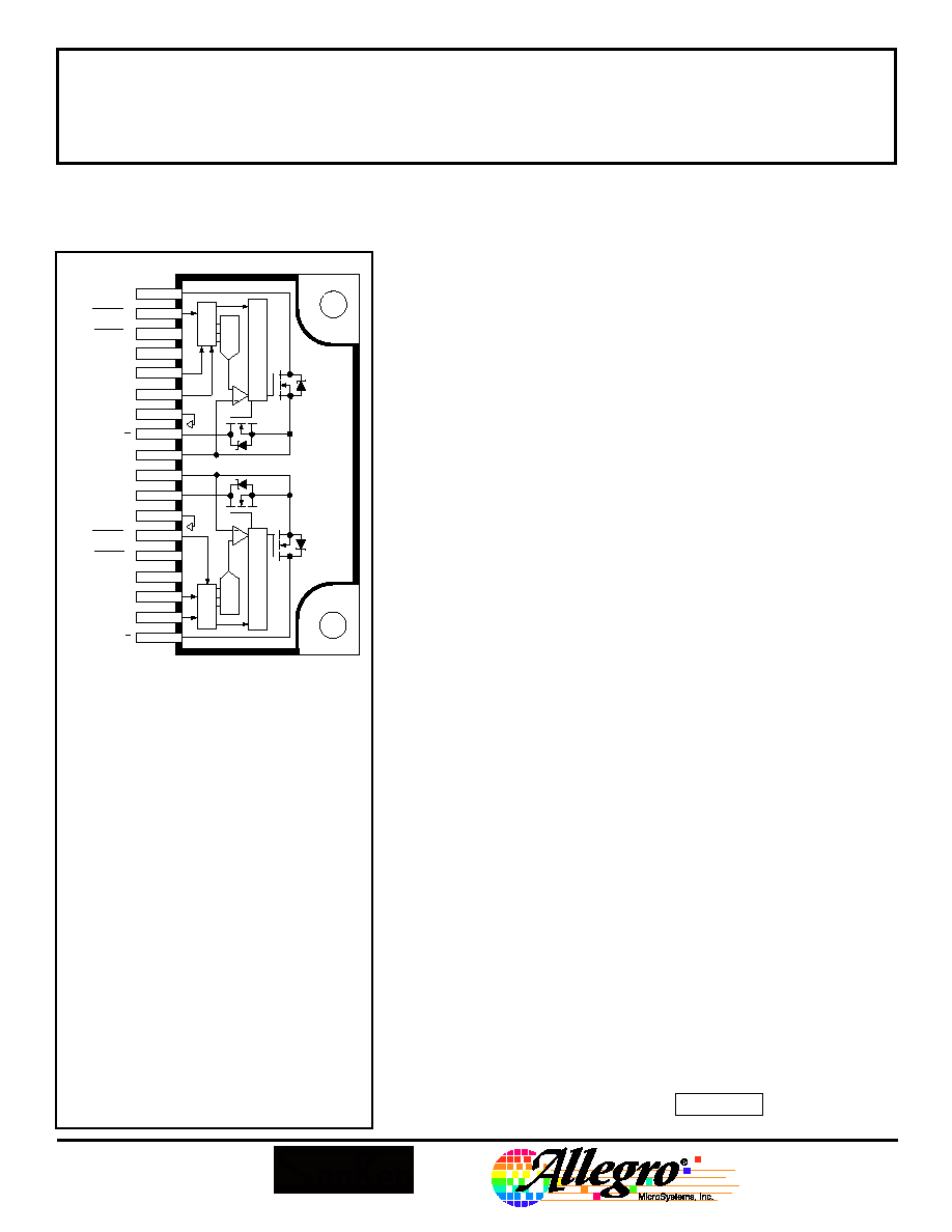
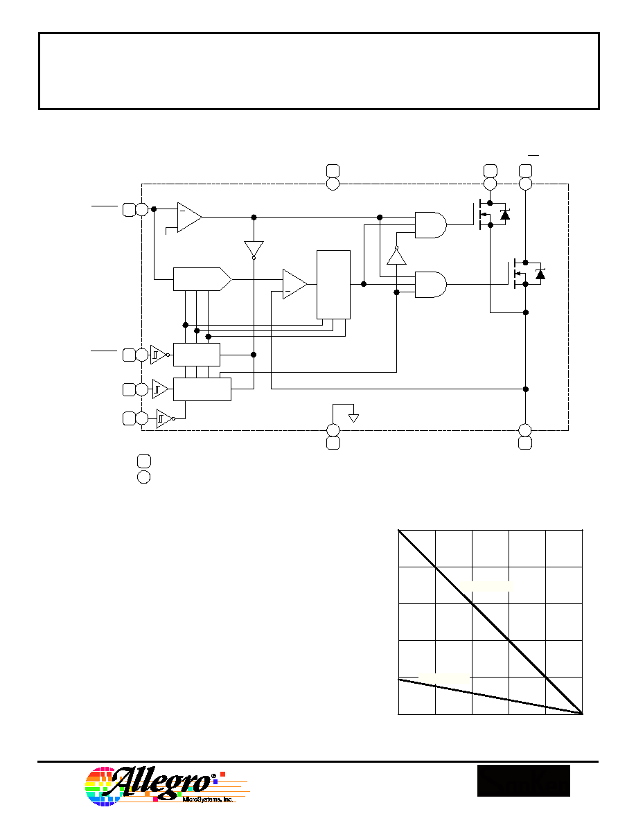
FUNCTIONAL BLOCK DIAGRAM
Note that channels A and B are electrically isolated.
50
75
100
125
150
25
15
10
5
0
TEMPERATURE in
∞
C
20
25
Dwg. GK-018-1
ALLOWABLE PACKAGE POWER DISSIPATION in WATTS
R = 5.0
∞
C/W
JM
R = 28
∞
C/W
JA
ALLOWABLE PACKAGE
POWER DISSIPATION
PROGRAMMABLE
PWM OFF TIMER
NOISE FILTER
+
D/A
LATCHES
SHIFT REG
12
7
GROUND
14
3
Dwg. FK-006
+
15
10
18
11
4
8
9
1
V
DD
SENSE
CONTROL
SUPPLY
OUT
A/B
OUT
A/B
REF/ENABLE
CHANNEL A PIN NUMBERS
CHANNEL B PIN NUMBERS
V ≠ 1
DD
PHASE
STROBE
DATA
CLOCK
13
2
17
6
16
5
ENABLE
V
REF
Copyright © 1995, 1998 Allegro MicroSystems, Inc.
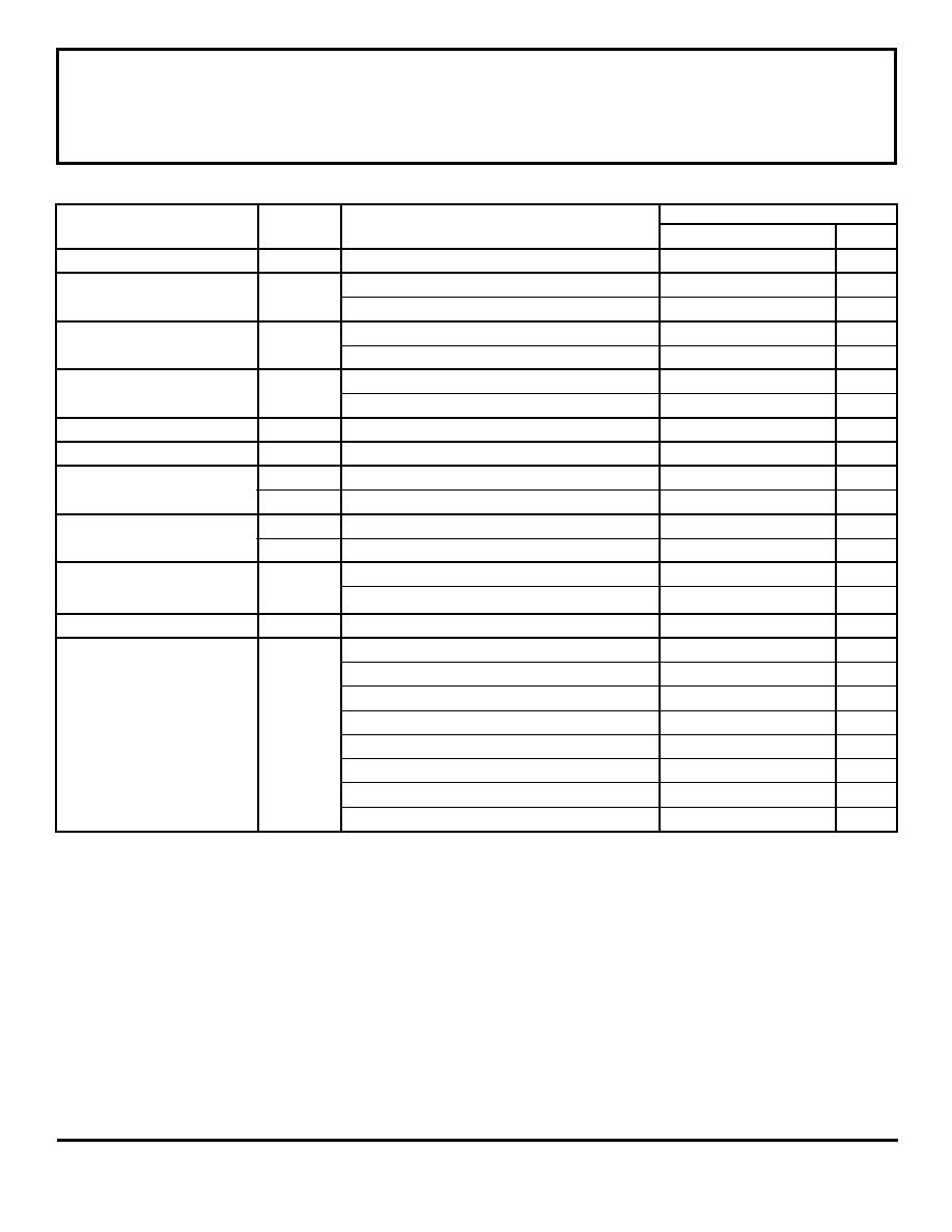
DC ELECTRICAL CHARACTERISTICS at T
A
= +25
∞
C, V
DD
= 5 V unless otherwise noted.
Limits
Characteristic
Symbol
Test Conditions
Min
Typ
Max
Units
FET Leakage Current
I
DSS
V
DS
= 100 V
--
--
4.0
mA
FET ON Voltage
V
DS(ON)
SLA7042M, I
OUT
= 1.2 A
--
--
800
mV
SLA7044M, I
OUT
= 3 A
--
--
855
mV
FET ON Resistance
r
DS(on)
SLA7042M, I
OUT
= 1.2 A
--
--
0.67
SLA7044M, I
OUT
= 3 A
--
--
0.285
Body Diode Forward Voltage
V
SD
SLA7042M, I
OUT
= ≠1.2 A
--
--
1.2
V
SLA7044M, I
OUT
= ≠3 A
--
--
1.6
V
Control Supply Voltage
V
DD
Operating
4.5
5.0
5.5
V
Control Supply Current
I
DD
Each controller, V
DD
= 5.5 V
--
--
7.0
mA
Logic Input Voltage
V
IN(1)
3.5
--
--
V
V
IN(0)
--
--
1.5
V
Logic Input Current
I
IN(1)
V
IN(1)
= V
DD
--
--
1.0
µ
A
I
IN(0)
V
IN(0)
= 0
--
--
≠1.0
µ
A
REF/ENABLE Input Voltage
V
REF/EN
DATA, CLOCK, STROBE, and OUT Enabled
0.4
--
2.5
V
DATA, CLOCK, STROBE, and OUT Disabled
V
DD
- 1
--
--
V
REF/ENABLE Input Current
I
REF/EN
0 V
V
REF/EN
5 V
--
--
±
1.0
µ
A
Step Reference
SRCR
DATA Input = 000X
--
0
--
%
Current Ratio
DATA Input = 001X
--
20
--
%
DATA Input = 010X
--
40
--
%
DATA Input = 011X
--
55.5
--
%
First Bit Entered (X) = Phase
DATA Input = 100X
--
71.4
--
%
Second Bit Entered = LSB
DATA Input = 101X
--
83
--
%
Last Bit Entered = MSB
DATA Input = 110X
--
91
--
%
DATA Input = 111X
--
100
--
%
NOTE: Negative current is defined as coming out of (sourcing) the specified device pin.
TYPICAL AC CHARACTERISTICS
at
T
A
= +25
∞
C, V
DD
= 5 V, I
OUT
= 1 A, Logic Levels are V
DD
and
Ground
PWM OFF Time
DATA Input = 001X ................................................................. 7
µ
s
DATA Input = 010X ................................................................. 7
µ
s
DATA Input = 011X ................................................................. 9
µ
s
DATA Input = 100X ................................................................. 9
µ
s
DATA Input = 101X ................................................................. 9
µ
s
DATA Input = 110X ................................................................ 11
µ
s
DATA Input = 101X ................................................................ 11
µ
s
Output RiseTime
t
r
10% to 90% ........................................................................... 0.5
µ
s
Output Fall Time
t
f
90% to 10% ........................................................................... 0.1
µ
s
Strobe-to-Output Switching Time
t
pd
50% to 50% ........................................................................... 0.7
µ
s
SLA7042M
AND
SLA7044M
MICROSTEPPING,
UNIPOLAR PWM, HIGH-CURRENT
MOTOR CONTROLLER/DRIVERS
SLA7042M
AND
SLA7044M
MICROSTEPPING,
UNIPOLAR PWM, HIGH-CURRENT
MOTOR CONTROLLER/DRIVERS
115 Northeast Cutoff, Box 15036
Worcester, Massachusetts 01615-0036 (508) 853-5000
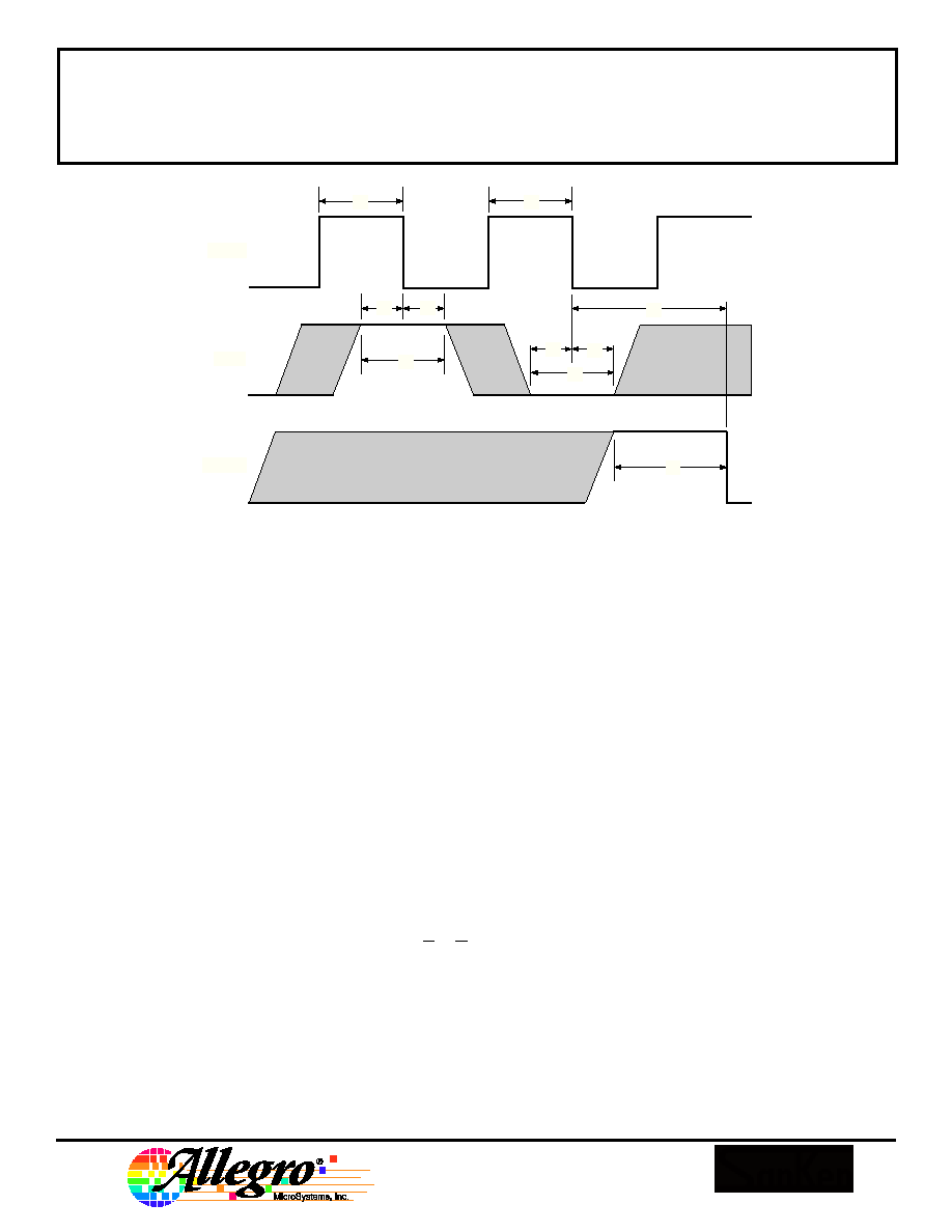
TM
CLOCK
DATA
STROBE
A
B
D
F
E
C
D
A
B
C
Dwg. WK-002
SERIAL PORT TIMING CONDITIONS
(T
A
= +25
∞
C, Logic Levels are V
DD
and Ground)
A. Minimum Data Active Time Before Clock Falling Edge (Data Set-Up Time) ........... 150 ns
B. Minimum Data Active Time After Clock Falling Edge (Data Hold Time) .................. 150 ns
C. Minimum Data Pulse Width ...................................................................................... 350 ns
D. Minimum Clock Pulse Width .................................................................................... 350 ns
E. Minimum Time Between Clock and Strobe Falling Edges ....................................... 650 ns
F. Minimum Strobe Pulse Width ................................................................................... 500 ns
APPLICATIONS INFORMATION
The SLA7042M and SLA7044M modules integrate two
CMOS controller ICs and four NMOS FETs. Each half of the
device operates independently, although the CLOCK inputs
may be connected together and the STROBE inputs may be
connected together. Pulling V
REF/EN
low (<2.5 V) allows the 4-
bit shift registers to be serially loaded with motor phase and
output currrent ratioing data.
The first bit selects the motor phase (logic high = Output A
or B, logic low = Output A or B); the next three bits determine
the motor current ratio (eight steps, 0% to 100%). The internal
D/A converter, in conjunction with a current-sensing resistor
and input reference voltage, completes the microstepping
current control.
Pulling V
REF/EN
high (within 1 V of V
DD
) resets the shift
register and latches to turn the MOS drivers OFF and inhibits
the serial DATA input.
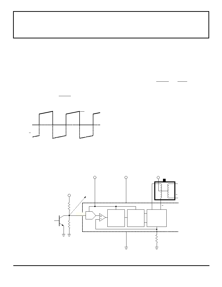
FIGURE 2. PWM CONTROL (RUN MODE)
Dwg. EK-011
R1
V
V b
CONTROL
LOGIC
S
V
BB
DD
DRIVE
R 2
R
A
A
B
B
REF/EN
V
PWM
OFF-TIME
CONTROL
SENSE
SERIAL DATA
D/A
ÿ
TO CHANNEL B
ENABLE
DATA
SERIAL DATA INPUT ENABLE
In a minimum-component application, a voltage divider
provides V
REF/EN
and an npn transistor provides the
required pull-down to enable the serial data input as
shown in Figure 2.
I
OUT
max
R
2
∑
V
b
R
1
+ R
2
3 ∑ R
S
µ
P STEPPER MOTOR CONTROL
Alternative REFERENCE/ENABLE input configura-
tions provide for more complete motor control. A tri-state
logic element and a voltage divider allows a fixed refer-
ence voltage, with both output disable and data enable
functions. Complete
µ
P control is usually accomplished
with a D/A converter as shown in Figure 3. Here, digital
control provides an output disable (>V
DD
- 1 V), V
REF
, and
V
EN
(<2.5 V).
SLA7042M
AND
SLA7044M
MICROSTEPPING,
UNIPOLAR PWM, HIGH-CURRENT
MOTOR CONTROLLER/DRIVERS
Dwg. WK-001
PHASE A
PHASE A
0
I
OUT
REGULATING THE PWM OUTPUT CURRENT
The output current (and motor coil current) waveform
is illustrated in Figure 1. Setting the maximum PWM
current trip point to meet the specified full-step running
current for the motor, I
OUT
max (DATA input = 111X =
100% ratio), requires only a current-sensing resistor, R
S
,
and an input reference voltage, V
REF/EN
, between 0.4 V
and 2.5 V.
I
OUT
max
V
REF/EN
3 ∑ R
S
FIGURE 1. PHASE A COIL CURRENT WAVEFORM