 | –≠–ª–µ–∫—Ç—Ä–æ–Ω–Ω—ã–π –∫–æ–º–ø–æ–Ω–µ–Ω—Ç: SLA7052M | –°–∫–∞—á–∞—Ç—å:  PDF PDF  ZIP ZIP |
Data Sheet
28210.1B*
UNIPOLAR STEPPER-MOTOR
TRANSLATOR/PWM DRIVER
Combining low-power CMOS logic with high-current, high-voltage
power FET outputs, the SLA7052M translator/driver provides complete
control and drive for a two-phase unipolar stepper motor with internal
fixed off time, pulse-width modulation (PWM) control of the output
current in a power multi-chip module (PMCMTM).
The CMOS logic section provides the sequencing logic, direction,
full/half-step control, synchronous/asynchronous PWM operation, and
a "sleep" function. The minimum CLOCK input is an ideal fit for
applications where a complex µP is unavailable or overburdened. TTL
or LSTTL may require the use of appropriate pull-up resistors to ensure
a proper input-logic high. For PWM current control, the maximum
output current is determined by the user's selection of a reference
voltage and sensing resistor. The NMOS outputs are capable of sinking
up to 3 A and withstanding 46 V in the off state. Ground-clamp and
flyback diodes provide protection against inductive transients. Special
power-up sequencing is not required.
Full-step (2 phase) and half-step operation are externally selectable.
Two-phase drive energizes two adjacent phases in each detent position
(AB-BC-CD-DA). This sequence mode offers an improved torque-
speed product, greater detent torque, and is less susceptable to motor
resonance. Half-step excitation alternates between the one-phase and
two-phase modes (A-AB-B-BC-C-CD D-DA), providing an eight-step
sequence.
The SLA7052M is supplied in an 18-pin single in-line power-tab
package with leads formed for vertical mounting (suffix LF871) or
horizontal mounting (suffix LF872). The tab is at ground potential and
needs no insulation. For high-current or high-frequency applications,
external heat sinking may be required. This device is rated for continu-
ous operation between -20∞C and +85∞C.
F
EATURES
3 A Output Rating
Internal Sequencer for Full or Half-Step Operation
PWM Constant-Current Motor Drive
Cost-Effective, Multi-Chip Solution
100 V, Avalanche-Rated NMOS
Low
r
DS(on)
NMOS Outputs (150 m
typical)
Advanced, Improved Body Diodes
Half-Step and Full-Step Unipolar Drive
Inputs Compatible with 3.3 V or 5 V Control Signals
Sleep Mode
Internal Clamp Diodes
Always order by complete part number, e.g., SLA7052MLF871 .
A
BSOLUTE
M
AXIMUM
R
ATINGS
Driver Supply Voltage, V
BB
................. 46 V
Load Supply Voltage, V
M
................... 46 V
Output Current, I
O
............................ 3.0 A*
Logic Supply Voltage, V
DD
................ 7.0 V
Logic Input Voltage Range,
V
I
........................... -0.3 V to V
DD
+ 0.3 V
Sense Voltage, V
S
........................ ±2.0 V
Reference Input Voltage Range,
V
REF ...................................
-0.3 V to V
DD
+ 0.3 V
Package Power Dissipation,
P
D
........................................ See Graph
Junction Temperature, T
J
............. +150∞C
Operating Temperature Range,
T
A
................................. -20∞C to +85∞C
Storage Temperature Range,
T
S
............................... -30∞C to +150∞C
* Output current rating may be limited by duty cycle,
ambient temperature, and heat sinking. Under any set of
conditions, do not exceed the specified current rating or
junction temperature.
Internal filtering provides protection against transients
during the first 1 µs of the current-sense pulse.
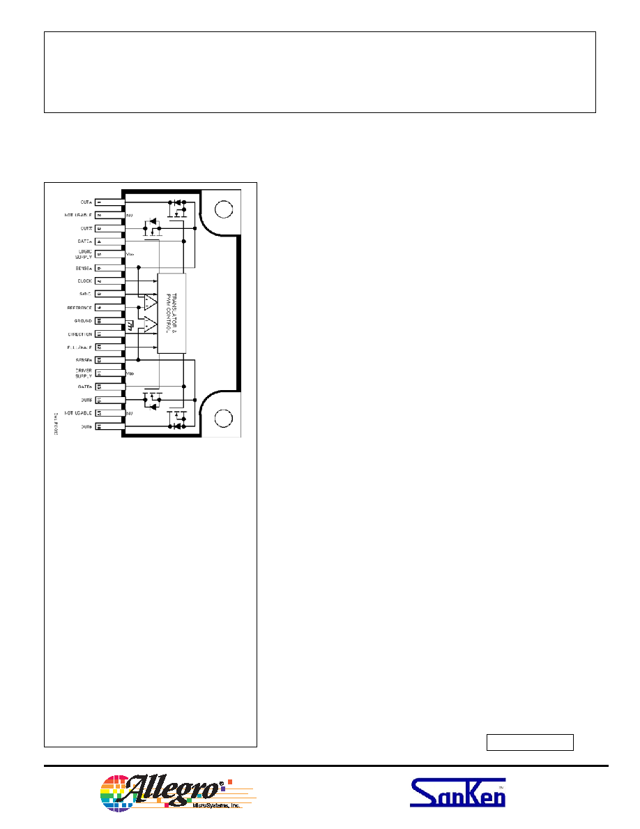
SLA7052M
Motor
Driver
Sanken Power Devices
from Allegro MicroSystems
115 Northeast Cutoff, Box 15036
Worcester, Massachusetts 01615-0036 (508) 853-5000
SLA7052M
UNIPOLAR STEPPER-MOTOR
TRANSLATOR/PWM DRIVER
2
Motor
Driver
Functional block diagram
Copyright © 2003, 2004 Allegro MicroSystems, Inc.
Recommended operating conditions
Load Supply Voltage, V
BB
.................................. 10 to 44 V
Logic Supply Voltage, V
DD
............................ 3.0 V to 5.5 V
Reference Input Voltage, V
REF
...................... 0.1 V to 1.0 V
Tab Temperature (no heat sink), T
T
...................... <100∞C
SLA7052M
UNIPOLAR STEPPER-MOTOR
TRANSLATOR/PWM DRIVER
www.allegromicro.com
3
Motor
Driver
Electrical characteristics: unless otherwise noted at T
A
= +25∞C, V
BB
= 24 V, V
DD
= 5.0 V.
Limits
Characteristic
Symbol
Test Conditions
Min.
Typ.
Max.
Units
Output drivers
Driver Supply Volt. Range
V
BB
Operating
10
--
44
V
Drain-Source Breakdown
V
(BR)DS
V
BB
= 44 V, I
D
= 1 mA
100
--
--
V
Output On Resistance
r
DS(on)
I
O
= 3.0 A
--
150
270
m
Body Diode Forward Volt.
V
F
I
F
= 3.0 A
--
1.5
2.3
V
Driver Supply Current
I
BB
--
--
15
mA
V
REF
> 2.0 V (sleep mode)
--
--
100
µA
Control logic
Logic Supply Volt. Range
V
DD
Operating
3.0
5.0
5.5
V
Logic Input Voltage
V
IH
0.75V
DD
--
--
V
V
IL
--
--
0.25V
DD
V
Logic Input Current
I
IH
--
±1.0
--
µA
I
IL
--
±1.0
--
µA
Max. Clock Frequency
f
clk
100*
--
--
kHz
PWM Off Time
t
off
--
12
--
µs
PWM Min. On Time
t
on(min)
--
5.0
--
µs
Ref. Input Voltage Range
V
REF
Operating
0.0
--
1.5
V
Sleep mode
2.0
--
--
V
Ref. Input Current
I
REF
--
±10
--
µA
Sense Voltage
V
S
Trip point
--
V
REF
--
V
Propagation Delay Time
t
PLH
Clock rising edge to output on
--
2.5
--
µs
t
PHL
Clock rising edge to output off
--
2.0
--
µs
Logic Supply Current
I
DD
--
--
3.0
mA
Typical values are given for circuit design information only.
*Operation at a clock frequency greater than the specified minimum value is possible but not warranted.
115 Northeast Cutoff, Box 15036
Worcester, Massachusetts 01615-0036 (508) 853-5000
SLA7052M
UNIPOLAR STEPPER-MOTOR
TRANSLATOR/PWM DRIVER
4
Motor
Driver
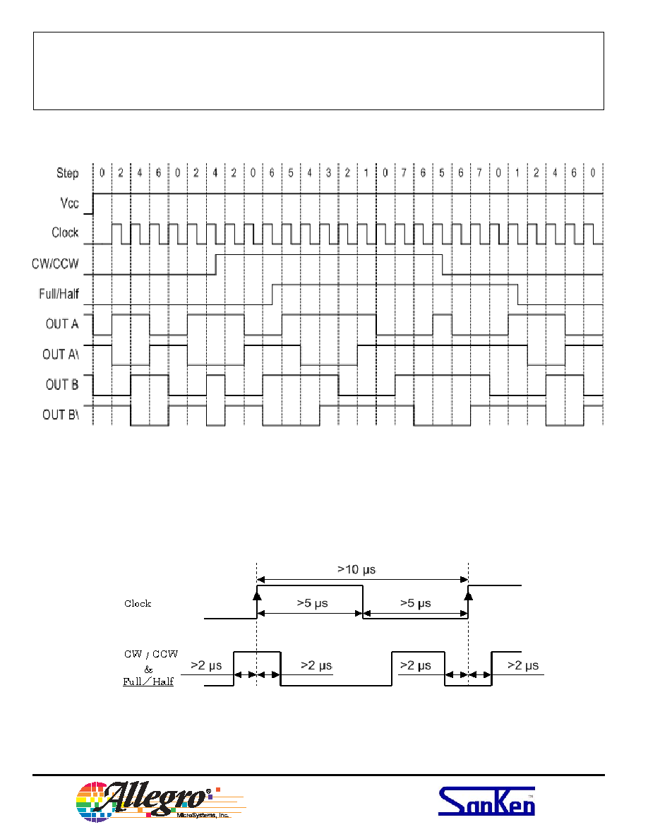
Timing chart
Logic input timing

SLA7052M
UNIPOLAR STEPPER-MOTOR
TRANSLATOR/PWM DRIVER
www.allegromicro.com
5
Motor
Driver
Functional description
Device operation.
The SLA7052M is a complete
stepper-motor driver with built-in translator for easy
operation with minimal control lines. It is designed to
operate unipolar stepper motors in full-step or half-step
modes. The current in each pair of outputs, all n-channel
MOSFETs, is regulated with internal fixed off-time pulse-
width modulated (PWM) control circuitry.
When a step command signal occurs on the clock input
the translator automatically sequences to the next step.
Clock (step) input.
A low-to-high transition on the
clock input sequences the translator and advances the
motor one increment. The hold state is done by stopping
the CLOCK input regardless of the input level
Full/half-step select.
This logic-level input sets the
translator step mode. A logic low is two-phase, full step; a
logic high is half step. Changes to this input do not take
effect until the rising edge of the clock input.
CW/CCW (direction) input.
This logic-level input sets
the translator step direction. Changes to this input do not
take effect until the rising edge of the clock input.
Internal PWM current control.
Each pair of outputs is
controlled by a fixed off-time PWM current-control circuit
that limits the load current to a desired value (I
TRIP
).
Initially, an output is enabled and current flows through
the motor winding and R
S
. When the voltage across the
current-sense resistor equals the reference voltage, the
current-sense comparator resets the PWM latch, which
turns off the driver for the fixed off time during which the
load inductance causes the current to recirculate for the off
time period. The driver is then re-enabled and the cycle
repeats.
Synchronous operation mode.
This function pre-
vents occasional motor noise during a "hold" state, which
normally results from asynchronous PWM operation of
both motor phases. A logic high at the SYNC input is
synchronous operation; a logic low is asynchronous
operation. The use of synchronous operation during
normal stepping is not recommended because it produces
less motor torque and can cause motor vibration due to
stair-case current.
Sleep mode.
Applying a voltage greater than 2 V to the
REF pin disables the outputs and puts the motor in a free
state (coast). This function is used to minimize power
consumption when not in use. It disables much of the
internal circuitry including the output MOSFETs and
regulator. When coming out of sleep mode, wait 100 µs
before issuing a step command to allow the internal
circuitry to stabilize.
115 Northeast Cutoff, Box 15036
Worcester, Massachusetts 01615-0036 (508) 853-5000
SLA7052M
UNIPOLAR STEPPER-MOTOR
TRANSLATOR/PWM DRIVER
6
Motor
Driver
Applications information
Layout.
The printed wirting board should use a heavy ground
plane.
For optimum electrical and thermal performance, the
driver should be soldered directly into the board.
The driver supply terminal, VBB, should be decoupled
with an electrolytic capacitor placed as close to the device
as possible.
To avoid problems due to capacitive coupling of the
high dv/dt switching transients, route the high-level, output
traces away from the sensitive, low-level logic traces.
Always drive the logic inputs with a low source impedance
to increase noise immunity.
Grounding.
A star ground system located close to the
driver is recommended. The logic supply return and the
driver supply return should be connected together at only a
single point -- the star ground.
Logic supply voltage, V
DD
.
Transients at this terminal
should be held to less than 0.5 V to avoid malfunctioning
operation. Both V
BB
and V
DD
may be turned on or off
separately.
Logic inputs.
Unused logic inputs (CW/CCW, FULL/
HALF, or SYNC) must be connected to either ground or
the logic supply voltage.
Current sensing.
To minimize inaccuracies caused by
ground-trace IR drops in sensing the output current level,
the current-sense resistor, R
S
, should have an independent
ground return to the star ground of the device. This path
should be as short as possible. For low-value sense
resistors, the IR drops in the printed wiring board sense
resistor's traces can be significant and should be taken into
account. The use of sockets should be avoided as they can
introduce variation in R
S
due to their contact resistance.
PWM current control.
The maximum value of current
limiting (I
TRIP
) is set by the selection of R
S
and the voltage
at the REF input with a transconductance function ap-
proximated by:
I
TRIP
= V
REF
/R
S
The required V
REF
should not be less than 0.1 V. If it is,
R
S
should be increased for a proportionate increase in
V
REF
.
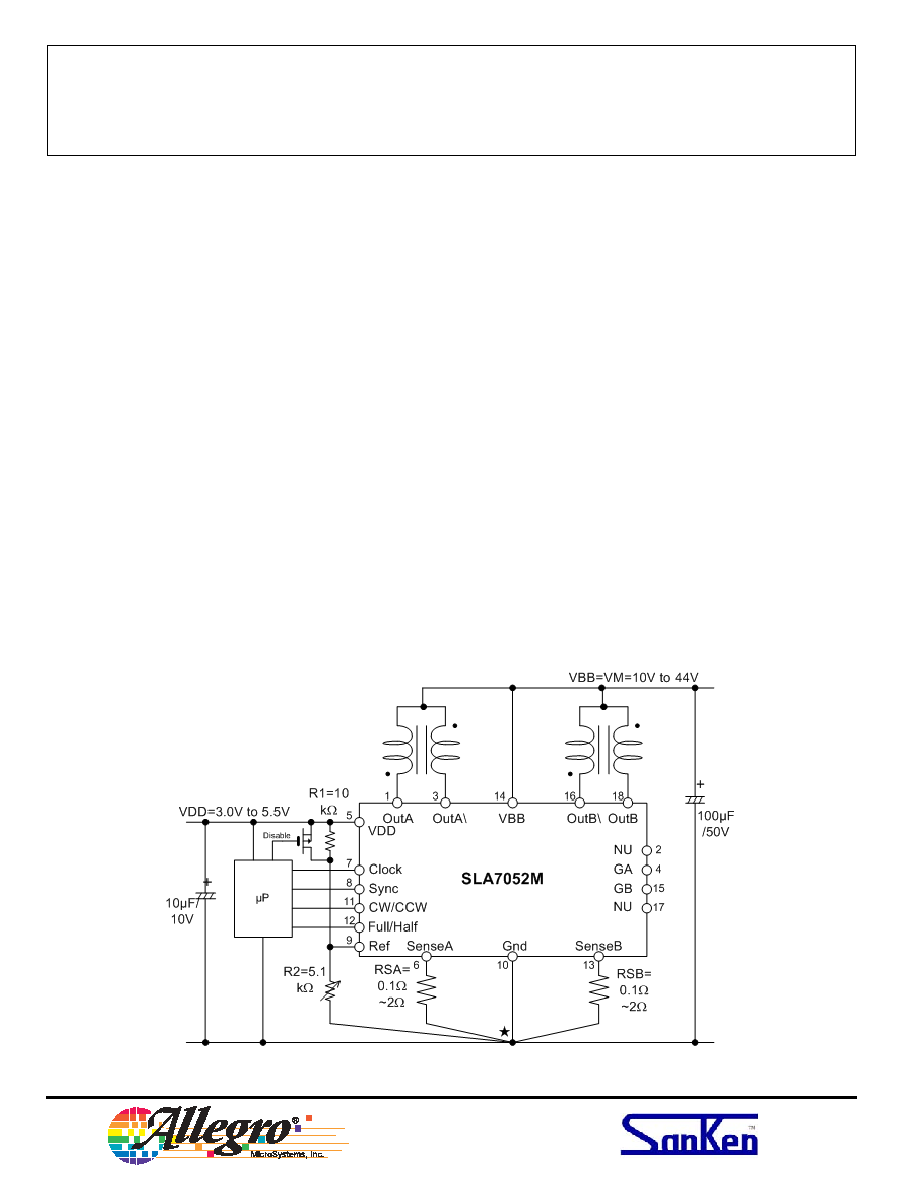
Typical application
SLA7052M
UNIPOLAR STEPPER-MOTOR
TRANSLATOR/PWM DRIVER
www.allegromicro.com
7
Motor
Driver
Applications Information (cont'd)
Continuous
Discontinuous
mode
mode
Normalized FET on resistance
Sync. signal generator
Reference voltage.
In the Typical Application shown,
resistors R
1
and R
2
set the reference voltage as:
V
REF
=
(V
DD
x R
2
)/(R
1
+ R
2
)
The trimming of R
2
allows for the resistor tolerances
and REF input current. The sum of R
1
+R
2
should be less
than 50 k
to minimize the effect of I
REF
.
Minimum output current.
The SLA7052M uses fixed
off-time PWM current control. Due to internal logic and
switching delays, the actual load current peak will be
slightly higher than the calculated I
TRIP
value (especially
for low-inductance loads). These delays, plus the mini-
mum recommended V
REF
, limit the minimum value the
current-control circuitry can regulate. An application with
this device should maintain continuous PWM control in
order to obtain optimum torque out of the motor. The
boundary of the load current (I
O(min)
) between continuous
and discontinuous operation is:
I
O(min)
= [(V
M
+ V
SD
)/R
m
] x [(1/e
toff/[Rm x Lm]
) - 1]
where V
M
= load supply voltage
V
F
= body diode forward voltage
R
m
= motor winding resistance
t
off
= PWM off time
L
m
= motor winding inductance
To produce zero current in a motor, the REF input
should be pulled above 2 V, turning off all drivers.
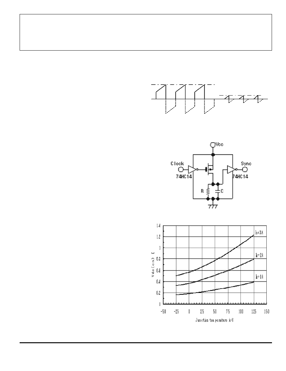
Synchronous operation mode.
If an external signal
is not available to control the synchronous operation
mode, a simple circuit can keep the SYNC input low while
the CLOCK input is active; the SYNC input will go high
(synchronous operation) when the CLOCK input stays low
("hold"). The RC time constant determines the sync
trransition timing.
Temperature effects on FET outputs.
Analyzing
safe, reliable operation includes a concern for the relation-
ship of NMOS on resistance to junction temperature.
Device package power calculations must include the
increase in on resistance (producing higher on voltages)
caused by increased operating junction temperatures. The
figure provides a normalized on-resistance curve, and all
thermal calculations should consider increases from the
115 Northeast Cutoff, Box 15036
Worcester, Massachusetts 01615-0036 (508) 853-5000
SLA7052M
UNIPOLAR STEPPER-MOTOR
TRANSLATOR/PWM DRIVER
8
Motor
Driver
Applications Information (cont'd)
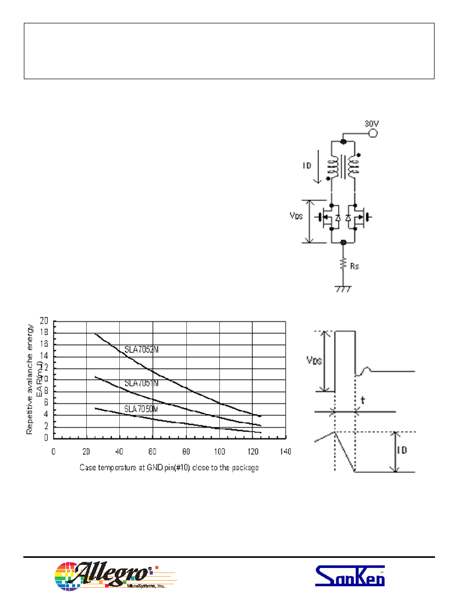
Allowable avalanche energy
Waveforms during avalanche breakdown
given +25∞C limits, which may be caused by internal
heating during normal operation.
These power MOSFET outputs feature an excellent
combination of fast switching, ruggedized device design,
low on resistance, and cost effectiveness.
Avalanche energy capability.
There is a surge voltage
expected when the output MOSFET turns off, and this
voltage may exceed the MOSFET breakdown voltage
(V
(BR)DS
). However, the MOSFETs are avalanche type
and as long as the energy (E
(AV)
), which is imposed on the
MOSFET by the surge voltage, is less than the maximum
allowable value, it is considered to be within its safe
operating area. Note that the maximum allowable ava-
lanche energy is reduced as a function of temperature.
In application, the avalanche energy (E
(AV)
) dissipated
by the MOSFET is approximated as
E
(AV)
= V
DS(AV)
x 1/2 x I
D
x t
Output circuit for avalanche energy
calculations
SLA7052M
UNIPOLAR STEPPER-MOTOR
TRANSLATOR/PWM DRIVER
www.allegromicro.com
9
Motor
Driver
Terminal list
Terminal
Pin
Name
Terminal Description
1
OUT
A
Driver output for phase A
2
NU
Not usable
3
OUT
A
\
Driver output for phase A\
4
GATE
A
Phase A MOSFET Gate
5
V
DD
Logic power supply
6
SENSE
A
Phase A current sense
7
CLOCK
Step clock input
8
SYNC
Synchronous PWM control input
9
REF
Current set & "sleep" control
10
GND
Supply negative return
11
CW/CCW
Forward/reverse logic control input
12
FULL/HALF
Full step/half step logic control input
13
SENSE
B
Phase B current sense
14
V
BB
Driver power supply
15
GATE
B
Phase B MOSFET Gate
16
OUT
B
\
Driver output for phase B\
17
NU
Not usable
18
OUT
B
Driver output for phase B
The products described herein are manufactured in Japan by
Sanken Electric Co., Ltd. for sale by Allegro MicroSystems, Inc.
Sanken and Allegro reserve the right to make, from time to time,
such departures from the detail specifications as may be required to
permit improvements in the performance, reliability, or
manufacturability of its products. Therefore, the user is cautioned to
verify that the information in this publication is current before placing
any order.
When using the products described herein, the applicability and
suitability of such products for the intended purpose shall be reviewed
at the users responsibility.
Although Sanken undertakes to enhance the quality and reliability of
its products, the occurrence of failure and defect of semiconductor
products at a certain rate is inevitable.
Users of Sanken products are requested to take, at their own risk,
preventative measures including safety design of the equipment or
systems against any possible injury, death, fires or damages to society
due to device failure or malfunction.
Sanken products listed in this publication are designed and intended
for use as components in general-purpose electronic equipment or
apparatus (home appliances, office equipment, telecommunication
equipment, measuring equipment, etc.). Their use in any application
requiring radiation hardness assurance (e.g., aerospace equipment) is
not supported.
When considering the use of Sanken products in applications where
higher reliability is required (transportation equipment and its control
systems or equipment, fire- or burglar-alarm systems, various safety
devices, etc.), contact a Sanken sales representative to discuss and
obtain written confirmation of your specifications.
The use of Sanken products without the written consent of Sanken in
applications where extremely high reliability is required (aerospace
equipment, nuclear power-control stations, life-support systems, etc.) is
strictly prohibited.
The information included herein is believed to be accurate and
reliable. Application and operation examples described in this
publication are given for reference only and Sanken and Allegro
assume no responsibility for any infringement of industrial property
rights, intellectual property rights, or any other rights of Sanken or
Allegro or any third party that may result from its use.
115 Northeast Cutoff, Box 15036
Worcester, Massachusetts 01615-0036 (508) 853-5000
SLA7052M
UNIPOLAR STEPPER-MOTOR
TRANSLATOR/PWM DRIVER
10
Motor
Driver
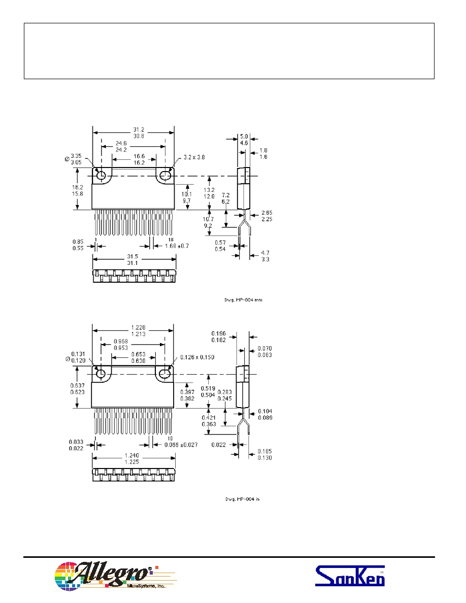
NOTES: 1. Exact body and lead configuration at vendor's option within limits shown.
2. Lead spacing tolerance is non-cumulative.
3. The shaded area is exposed heat spreader.
3. Recommended mounting hardware torque: 0.490 - 0.822 Nm.
4. Recommended use of metal-oxide-filled, alkyl-degenerated oil-base silicone grease: Dow Corning SC102,
Toshiba YG6260, Shin-Etsu G746, or equivalent.
SLA7052MLF871
Dimensions in inches
(for reference only)
Dimensions in millimeters
(controlling dimensions)
SLA7052M
UNIPOLAR STEPPER-MOTOR
TRANSLATOR/PWM DRIVER
www.allegromicro.com
11
Motor
Driver
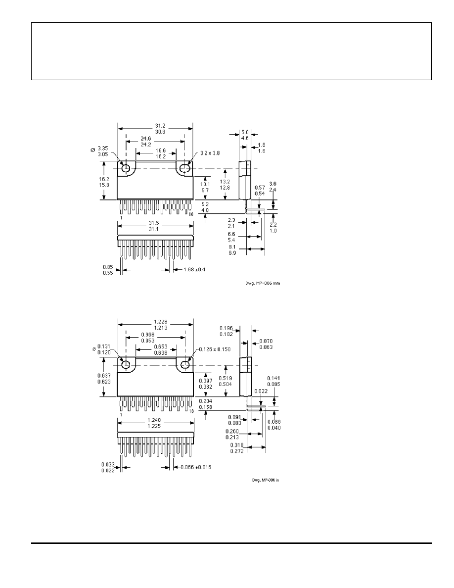
NOTES: 1. Exact body and lead configuration at vendor's option within limits shown.
2. Lead spacing tolerance is non-cumulative.
3. The shaded area is exposed heat spreader.
3. Recommended mounting hardware torque: 0.490 - 0.822 Nm.
4. Recommended use of metal-oxide-filled, alkyl-degenerated oil-base silicone grease: Dow Corning SC102,
Toshiba YG6260, Shin-Etsu G746, or equivalent.
SLA7052MLF872
Dimensions in inches
(for reference only)
Dimensions in millimeters
(controlling dimensions)
115 Northeast Cutoff, Box 15036
Worcester, Massachusetts 01615-0036 (508) 853-5000
SLA7052M
UNIPOLAR STEPPER-MOTOR
TRANSLATOR/PWM DRIVER
12
Motor
Driver
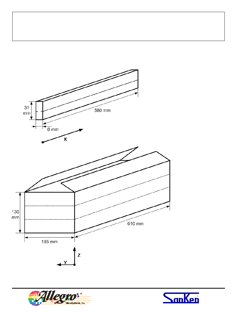
Packing information
20 sticks/tubes in Y direction;
3 layers of sticks/tubes in Z direction = 1080 devices per box.
18 devices per stick/tube.
A rubber stopper is provided at each end of the stick/tube.