 | –≠–ª–µ–∫—Ç—Ä–æ–Ω–Ω—ã–π –∫–æ–º–ø–æ–Ω–µ–Ω—Ç: STRG6632 | –°–∫–∞—á–∞—Ç—å:  PDF PDF  ZIP ZIP |
The STR-G6651 is specifically designed to satisfy the requirements
for increased integration and reliability in off-line quasi-resonant flyback
converters. This device incorporates the primary control and drive
circuit with a discrete avalanche-rated power MOSFET.
Cycle-by-cycle current limiting, under-voltage lockout with hyster-
esis, over-voltage protection, and thermal shutdown protects the power
supply during the normal overload and fault conditions. Over-voltage
protection and thermal shutdown are latched after a short delay. The
latch may be reset by cycling the input supply. Low-current startup and
a low-power standby mode selected from the secondary circuit completes
a comprehensive suite of features. The device is provided in a five-pin
over-molded TO-220 style package, affording dielectric isolation without
compromising thermal characteristics. Two lead forms are available
(with and without the suffix `-LF') to accommodate printed wiring board
layout or mechanical constraints.
Proven in substantial volumes, the STR-G6651 is a robust low-risk
solution for off-line power supplies particularly where management of
EMI at the source is a significant element of the system design.
FEATURES
I Quasi-Resonant Operation
I Output Power to 66 W
I Low-Loss, Pulse-Ratio-Control Standby Mode
I Temperature-Compensated Pulse-by-Pulse Over-Current Protection
I Latched Over-Voltage and Thermal Protection
I Under-Voltage Lockout with Hysteresis
I Active Low-Pass Filter for Enhanced Light-Load Stability
I Switched Attenuation of Leading-Edge Current-Sensing Signal
I Regulated Soft Gate Drive
I Adjustable Switching Speed for EMI Control
I Overmolded Five-Pin Package
OFF-LINE QUASI-RESONANT
FLYBACK SWITCHING REGULATOR
Always order by complete part number: STR-G6651 .
Data Sheet
28102.9A
TM
STR-G6651
ABSOLUTE MAXIMUM RATINGS
at T
A
= +25
∞
C
Control Supply Voltage, V
IN
. . . . . . . 35 V
Drain-Source Voltage, V
DS
. . . . . . . . 650 V
Drain Current, I
D
continuous . . . . . . . . . . . . . . . . . . 2.7 A
single-pulse, t
w
1 ms . . . . . . . . 7.2 A
Avalanche Energy, E
AS
single-pulse . . . . . . . . . . . . . . . 158 mJ
Over-Current Protection Voltage Range,
V
OCP
. . . . . . . . . . . . . . . -0.3 V to +6 V
Insulation RMS Voltage,
V
WM(RMS)
. . . . . . . . . . . . . . . . . . 2000 V
Package Power Dissipation, P
D
control (V
IN
x I
IN(ON)
) . . . . . . . . . 0.8 W
total . . . . . . . . . . . . . . . . . . . See Graph
FET Channel Temperature, T
J
. . . +150
∞
C
Internal Frame Temperature, T
F
. . +125
∞
C
Operating Temperature Range,
T
A
. . . . . . . . . . . . . . . -20
∞
C to +125
∞
C
Storage Temperature Range,
T
S
. . . . . . . . . . . . . . . -40
∞
C to +125
∞
C
SOURCE
DRAIN
OVERCURRENT
& FEEDBACK
GROUND
Dwg. PK-011
V
IN
1
2
3
4
5
UVLO
OVP
TSD
LATCH
OSC.
OCP
FDBK
SUPPLY
STR-G6651
OFF-LINE
QUASI-RESONANT FLYBACK
SWITCHING REGULATOR
115 Northeast Cutoff, Box 15036
Worcester, Massachusetts 01615-0036 (508) 853-5000
TM
Copyright © 1999, 2000 Allegro MicroSystems, Inc.
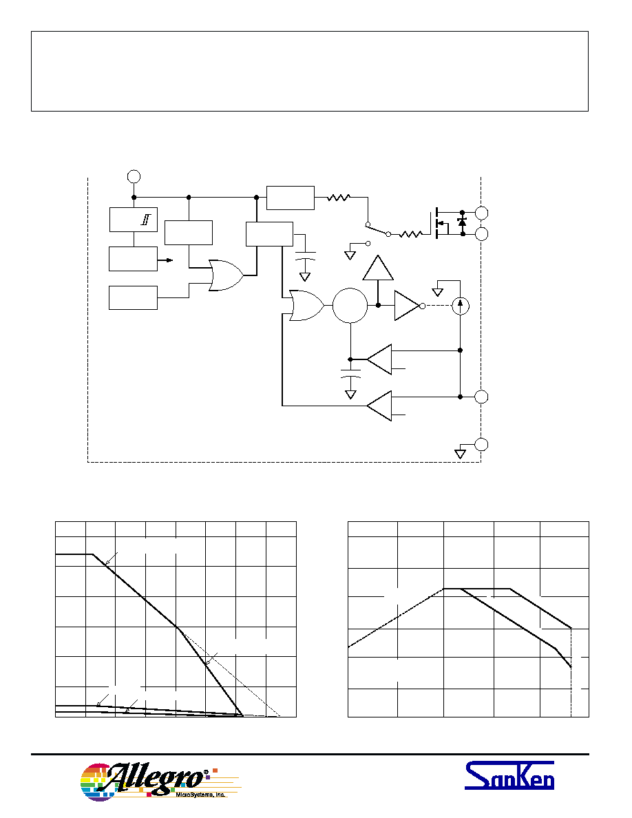
FUNCTIONAL BLOCK DIAGRAM
FEEDBACK &
OVER-CURRENT
PROTECTION
GROUND
V
IN
SOURCE
DRAIN
Dwg. FK-002-5
0.73 V
≠
≠
TSD
OVER-VOLT.
PROTECT
R
S
Q
REF.
FAULT
LATCH
4
1
2
1.45 V
UVLO
+
5
+
1.35 mA
3
DRIVE
REG.
OSC
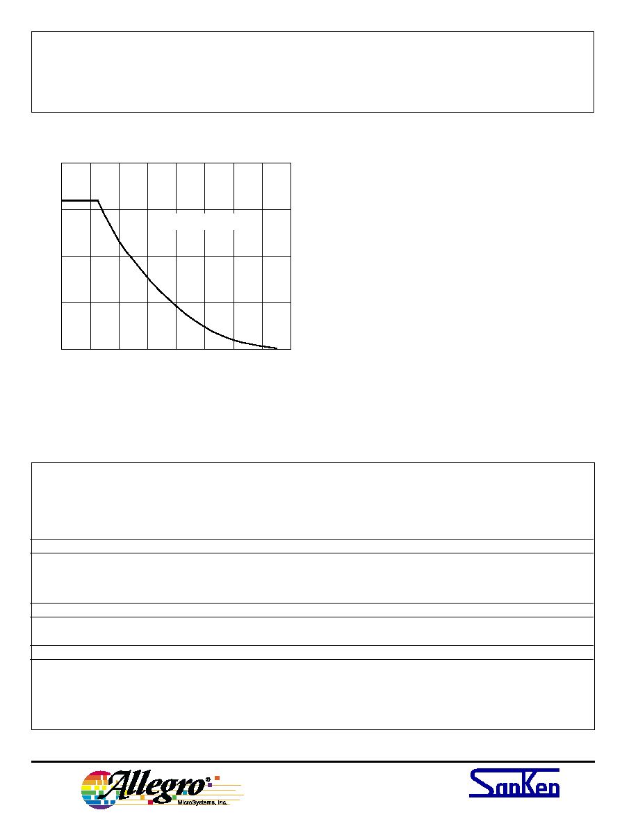
ALLOWABLE PACKAGE POWER DISSIPATION
MAXIMUM SAFE OPERATING AREA
30
20
10
20
60
100
1.5 W
140
LIMITED BY FRAME
TEMP. = +125
∞C MAX.
FREE AIR
27 W
0
TEMPERATURE in
∞C
ALLOWABLE PACKAGE POWER DISSIPATION in WATTS
MOUNTING SURFACE
TEMPERATURE
Dwg. GK-003-4
0.8 W
CONTROLLER
50
5
0.5
0.05
DRAIN-SOURCE VOLTAGE in VOLTS
DRAIN CURRENT in AMPERES
Dwg. GK-004-5
0.15
1.5
15
3.0
10
30
100
300
NO HEAT SINK
NATURAL COOLING
T
A
= +25
∞C
t
w
= 1 ms SINGLE PULSE
1000
t
w
= 0
.1 m
s S
IN
GL
E P
UL
SE
LIMITED BY V
DS
max
LIMITED
BY
r
DS(on)

STR-G6651
OFF-LINE
QUASI-RESONANT FLYBACK
SWITCHING REGULATOR
www.allegromicro.com
ELECTRICAL CHARACTERISTICS at T
A
= +25
∞
C, V
IN
= 18 V, V
DD
= 10 V, V
S
= 0, voltage mea-
surements are referenced to ground terminal (unless otherwise specified).
Limits
Characteristic
Symbol
Test Conditions
Min.
Typ.
Max.
Units
On-State Voltage
V
INT
Turn-on, increasing V
IN
14.4
16
17.6
V
Under-Voltage Lockout
V
INQ
Turn-off, decreasing V
IN
9.0
10
11
V
Over-Voltage Threshold
V
OVP(th)
Turn-off, increasing V
IN
20.5
22.5
24.5
V
Drain-Source Breakdown Voltage
V
(BR)DSS
I
D
= 300
µA
650
≠
≠
V
Drain Leakage Current
I
DSS
V
DS
= 650 V
≠
≠
300
µA
On-State Resistance
r
DS(on)
V
S
= 10 V, I
D
= 0.9 A, T
J
= +25
∞C
≠
≠
3.95
Maximum OFF Time
t
off
Drain waveform high
45
≠
55
µs
Minimum Pulse Duration for Input of
Quasi-Resonant Signals
t
w(th)
Drain waveform high
1
≠
≠
1.0
µs
Minimum OFF Time
t
off
Drain waveform high
1
≠
≠
1.5
µs
Feedback Threshold Voltage
V
FDBK
Drain waveform low to high
1
0.68
0.73
0.78
V
Oscillation synchronized
2
1.3
1.45
1.6
V
Over-Current Protection/Feedback
Sink Current
I
OCP/FB
V
OCP/FB
= 1.0 V
1.2
1.35
1.5
mA
Latch Holding Current
I
IN(OVP)
V
IN
reduced from 24.5 V to 8.5 V
≠
≠
400
mA
Latch Release Voltage
V
IN
I
IN
20 µA, V
IN
reduced from 24.5 V
6.6
≠
8.4
V
Switching Time
t
f
V
DD
= 200 V, I
D
= 0.9 A
≠
≠
250
ns
Supply Current
I
IN(ON)
Operating
3
≠
≠
30
mA
I
IN(OFF)
Increasing V
IN
prior to oscillation
≠
≠
100
µA
Insulation RMS Voltage
V
WM(RMS)
All terminals simultaneous refer-
2000
≠
≠
V
ence metal plate against backside
Thermal Shutdown
T
J
140
≠
≠
∞C
Thermal Resistance
R
JM
Output junction-to-mounting frame
≠
≠
1.63
∞C/W
Notes: Typical Data is for design information only.
1. Feedback is square wave, V
IM
= 2.2 V, t
h
= 1
µs, t
l
= 35
µs
2. For quasi-resonant operation, the input signal must be longer than t
w(th)
and greater than V
FDBK
3. Feedback is square wave, V
IM
= 2.2 V, t
h
= 4
µs, t
l
= 1
µs
STR-G6651
OFF-LINE
QUASI-RESONANT FLYBACK
SWITCHING REGULATOR
115 Northeast Cutoff, Box 15036
Worcester, Massachusetts 01615-0036 (508) 853-5000
TM
ALLOWABLE AVALANCHE ENERGY
200
100
0
60
100
140
50
STARTING CHANNEL TEMPERATURE in
∞C
ALLOWABLE AVALANCHE ENERGY in mJ
Dwg. GK-009-2
150
0
20
40
80
120
160
SINGLE PULSE
DRAIN CURRENT = 1.8 A
STR-G6600 Series
Drain-Source
Drain-Source
Output Breakdown Voltage
ON Resistance
at I
D
= 300
µ
A
at I
D
= 0.9 A
Part Number
V
(BR)DS
, Minimum
r
DS(on)
, Maximum
Output Power
For 100/120 V AC Input
STR-G6622
450 V
2.18
44 W ≠ 60 W
STR-G6624
450 V
0.92
98 W ≠ 130 W
For 110/120 V AC Input
STR-G6632
500 V
2.62
36 W ≠ 50 W
For 200/220 V AC Input
STR-G6651
650 V
3.95
66 W
STR-G6652
650 V
2.80
86 W
STR-G6653
650 V
1.95
120 W
STR-G6651
OFF-LINE
QUASI-RESONANT FLYBACK
SWITCHING REGULATOR
www.allegromicro.com
WARNING --
These devices are designed to be operated at lethal voltages and energy levels. Circuit
designs that embody these components must conform with applicable safety requirements. Precau-
tions must be taken to prevent accidental contact with power-line potentials. Do not connect
grounded test equipment.
The use of an isolation transformer is recommended during circuit development and breadboarding.
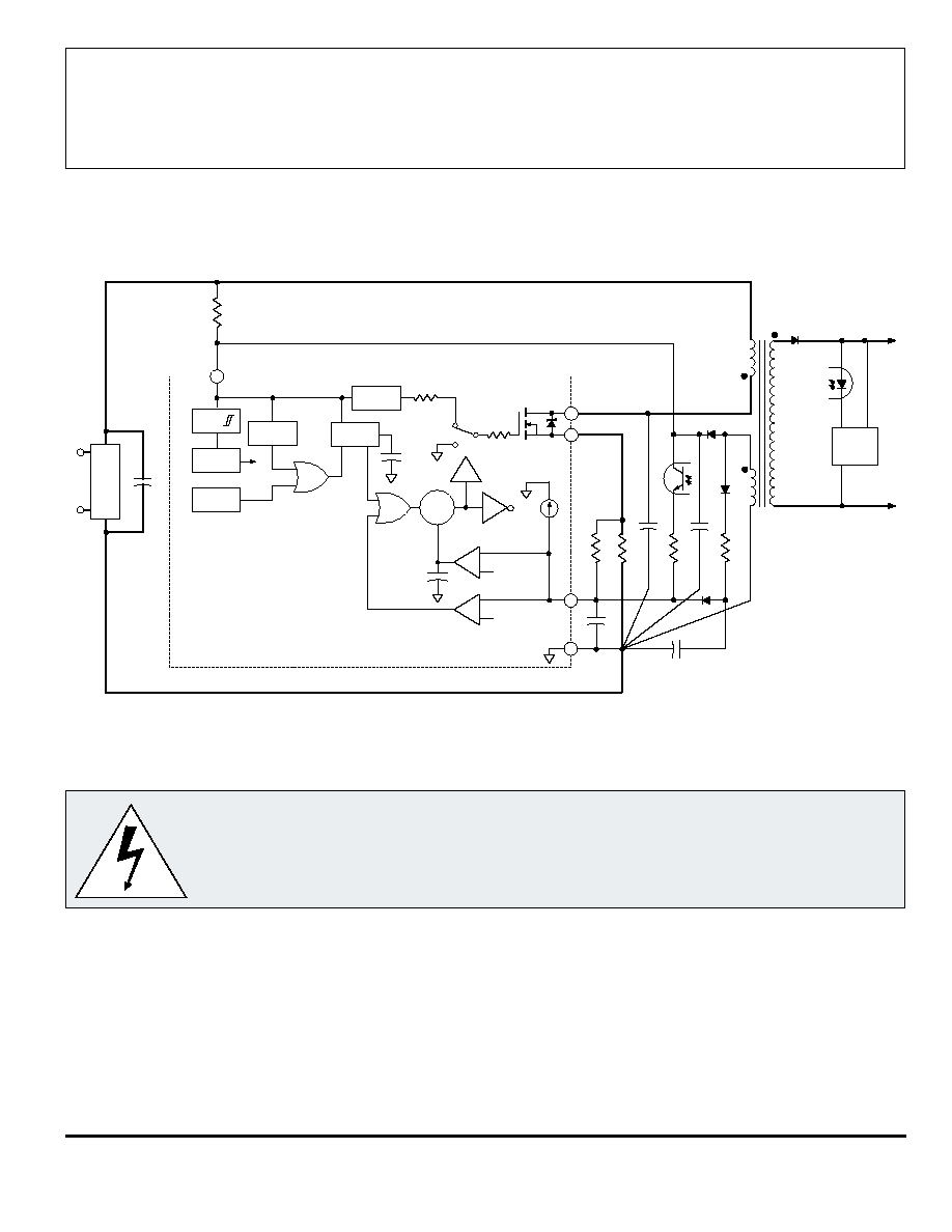
TYPICAL QUASI-RESONANT FLYBACK CONVERSION USING STR-G6651
WARNING: lethal potentials are present. See text.
Recommended mounting hardware torque:
4.34 - 5.79 lbf∑ft (6 ≠ 8 kg∑cm or 0.588 ≠ 0.784 Nm).
Recommended silicone grease:
Dow Corning SC102, Toshiba YG6260, Shin-Etsu G746., or equivalent
VOLTAGE
SENSE
+ OUTPUT
≠ OUTPUT
+
Dwg. EK-003-4A
#
0.73 V
≠
≠
TSD
OVER-VOLT.
PROTECT
R
S
Q
REF.
FAULT
LATCH
4
1
2
1.45 V
UVLO
+
5
+
OSC
1.35 mA
3
DRIVE
REG.
FULL-BRIDGE
RECTIFIER
AC INPUT
+