DISCONTINUED PRODUCT
-- FOR REFERENCE ONL
Y
Data Sheet
28102.11
The STR-S6525 is specifically designed to meet the requirement
for increased integration and reliability in off-line flyback converters
operating in a constant OFF-time mode. The device incorporates the
primary control and drive circuit with a discrete avalanche-rated high-
voltage power MOSFET.
Crucial system parameters such as maximum ON time and OFF
time are fixed during manufacture. Local control circuit decoupling and
layout are optimized within the device.
Cycle-by-cycle current limiting, soft start, under-voltage lock-out
with hysteresis, over-voltage protection, and thermal shutdown protect
the device during all normal and overload conditions. Over-voltage
protection, thermal shutdown, or an external fault signal be latched.
The dual requirements of dielectric isolation and low transient thermal
impedance and steady-state thermal resistance are satisfied in an over-
molded single-in-line power package.
Proven in substantial volumes, this device and its fixed-frequency
counterparts represents a significant advance in off-line SMPS reliability
growth and integration.
FEATURES
s
Constant OFF-Time Converter Operating Mode
s
Avalanche-Rated Power MOSFET Switch
s
Pulse-by-Pulse Current Limiting
s
Latched Over-Voltage and Thermal Protection
s
Maximum ON Time and OFF Time Set During Manufacture
s
Internal Under-Voltage Lockout with Hysteresis
s
Over-Molded SIP with Integral Isolated Heat Spreader
s
External Synchronization Capability
Always order by complete part number: STR-S6525 .
OFF-LINE SWITCHING REGULATOR
≠ WITH POWER MOSFET OUTPUT
STR-S6525
ABSOLUTE MAXIMUM RATINGS
Supply Voltage, V
IN
........................... 35 V
Drain-Source Voltage, V
DS
.............. 600 V
Continuous Drain Current, I
D
............ 6.0 A
1 ms Single-Pulse Drain Current,
I
DM
................................................. 24 A
Single-Pulse Avalanche Energy,
E
A
.............................................. 400 mJ
Feedback Input Current, I
FDBK
........ 20 mA
Fault-Latch Trig. Input Current, I
FL
1.0 mA
dc
25%, I
FLM
........................... -50 mA
Soft-Start Output Current, I
SS
....... -3.0 mA
Over-Current Protection Voltage,
V
OCP
............................................. 3.5 V
Insulation Voltage,V
WM(RMS)
........... 2000 V
Package Power Diss., P
D
........ See Graph
FET Junction Temperature, T
J
...... +150
∞
C
Internal Frame Temperature, T
F
... +125
∞
C
Operating Temperature Range,
T
A
............................... -20
∞
C to +125
∞
C
Storage Temperature Range,
T
stg
............................. -30
∞
C to +125
∞
C
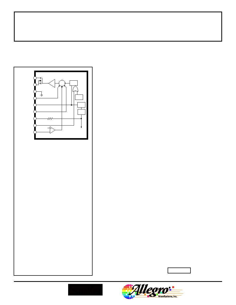
+
OVER-CURRENT
PROTECTION
SOURCE
DRAIN
UVLO
COMMON
V IN
Dwg. PK-002-1
SOFT START
FDBK
FAULT
LATCH
REF.
1
2
3
4
5
6
7
OSC.
R
S
FAULT
FAULT-LATCH
TRIGGER
8
9
SYNC
TM
STR-S6525
OFF-LINE
SWITCHING REGULATOR
115 Northeast Cutoff, Box 15036
Worcester, Massachusetts 01615-0036 (508) 853-5000
TM
FUNCTIONAL BLOCK DIAGRAM
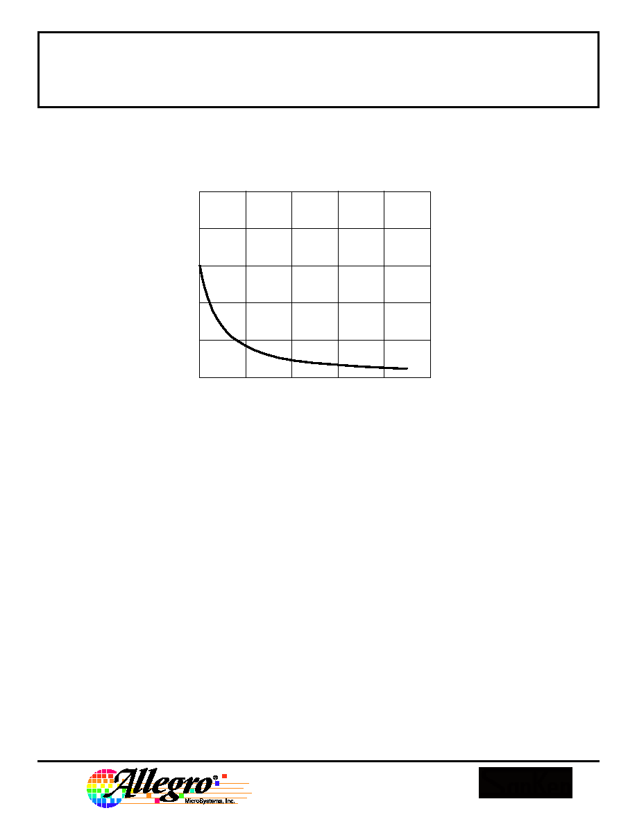
ALLOWABLE PACKAGE POWER DISSIPATION
MAXIMUM SAFE OPERATING AREA
60
40
20
20
60
100
3.2 W
140
LIMITED BY FRAME
TEMP. = +125
∞
C MAX.
RECOMMENDED MAX.
FRAME TEMP. = +100
∞
C
FREE AIR
54 W
0
TEMPERATURE in
∞
C
ALLOWABLE PACKAGE POWER DISSIPATION in WATTS
MOUNTING SURFACE
TEMPERATURE
Dwg. GK-003-2
SYNC
4
0.01
µ
F
OSC.
1 k
20 k
TSD
OVER-VOLT.
PROTECT
COMMON
3
R
S
Q
V
IN
FDBK
OVER-CURRENT
PROTECTION
SOURCE
DRAIN
Rton
REF.
FAULT
LATCH
5
1
2
9
6
Dwg. FK-002-1
TRIGGER
0.01
µ
F
2 k
SOFT
START
7
1000 pF
FAULT-LATCH
TRIGGER
8
Rtoff
0.75 V
+
UVLO
100
10
1.0
0.1
DRAIN-TO-SOURCE VOLTAGE in VOLTS
DRAIN CURRENT in AMPERES
Dwg. GK-004-4
0.3
3.0
30
3.0
10
30
100
300
LIMITED BY V max
DS
NO HEAT SINK
NATURAL COOLING
T = +25
∞
C
A
t = 1 ms SINGLE PULSE
w
t = 0.1 ms SINGLE PULSE
w
INFINITE HEAT SINK
1000
LIMITED
BY r
DS(on)
Copyright © 1994 Allegro MicroSystems, Inc.
600
400
200
0
60
100
140
100
STARTING CHANNEL TEMPERATURE in
∞
C
ALLOWABLE AVALANCHE ENERGY in mJ
Dwg. GK-009-1
300
500
0
20
40
80
120
160
SINGLE PULSE
DRAIN CURRENT = 5 A
SUPPLY VOLTAGE = 50 V
ALLOWABLE AVALANCHE ENERGY
ELECTRICAL CHARACTERISTICS
at T
A
= +25
∞
C, V
IN
= 18 V, voltage measurements are referenced to
Common (pin 3) (unless otherwise noted).
Limits
Characteristic
Symbol
Test Conditions
Min.
Typ. Max.
Units
On-State Voltage
V
INT
Turn-on, increasing V
IN
14.4
≠
17.6
V
Under-Voltage Lockout
V
INQ
Turn-off, decreasing V
IN
9.0
≠
11
V
Over-Voltage Threshold
V
OVP(th)
26
≠
31
V
FET Leakage Current
I
DSS
V
DS
= 600 V
≠
≠
300
µ
A
FET ON Resistance
r
DS(on)
V
GS
= 10 V, I
D
= 3 A
≠
1.0
1.25
Output Fall Time
t
f
V
DD
= 200 V, I
D
= 5 A, 10% to 90% V
DS
≠
≠
250
ns
Maximum ON Time
t
on
I
FDBK
= 0
27
≠
33
µ
s
Minimum OFF Time
t
off
50
≠
62
µ
s
Over-Current Threshold
V
OCP(th)
700
≠
800
mV
Feedback Threshold
V
FDBK(th)
≠
750
≠
mV
Soft-Start Voltage
V
SS
8.7
≠
9.7
V
Sync. Trigger Threshold Volt.
V
SYNC(th)
≠
3.0
≠
V
Fault-Latch Trig. Threshold
V
FL(th)
680
≠
880
mV
Fault-Latch Holding Current
I
INH
V
IN
reduced from 31 V to 8.5 V
≠
340
400
µ
A
Fault-Latch Reset Voltage
V
INQ
I
IN
20
µ
A, V
IN
reduced from 31 V
6.5
≠
8.5
V
Insulation RMS Voltage
V
WM(RMS)
All terminals simultaneous reference
2000
≠
≠
V
metal plate against backside
Supply Current
I
IN(ON)
Operating
9.0
≠
15
mA
I
IN(OFF)
Start up, V
IN
=14 V
≠
≠
200
µ
A
Thermal Shutdown
T
J
125
150
≠
∞
C
Thermal Resistance
R
JM
FET junction to mounting surface
≠
2.0
≠
∞
C/W
NOTES: Negative current is defined as coming out of (sourcing) the specified device terminal.
Typical Data is for design information only.
STR-S6525
OFF-LINE
SWITCHING REGULATOR
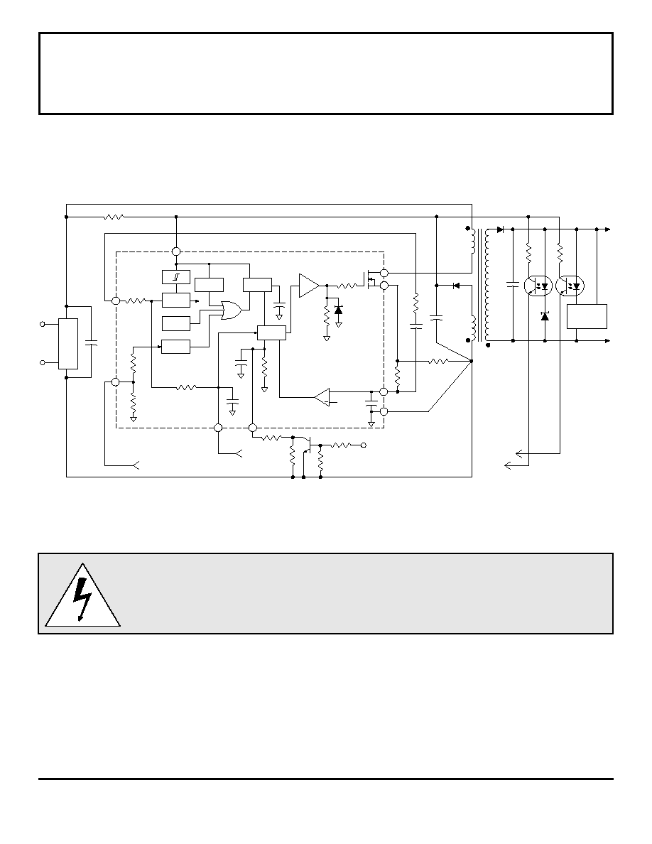
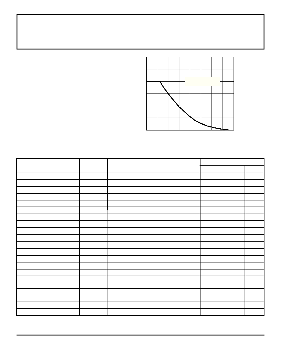
TYPICAL APPLICATION
WARNING: lethal potentials are present. See text.
APPLICATIONS INFORMATION
WARNING --
These devices are designed to be operated at lethal voltages and energy levels. Circuit
designs that embody these components must conform with applicable safety requirements. Precau-
tions must be taken to prevent accidental contact with power-line potentials. Do not connect
grounded test equipment.
The use of an isolation transformer is recommended during circuit development and breadboarding.
The power MOSFET outputs of these devices are similar to the International Rectifier type IRFBC40. These devices
feature an excellent combination of fast switching, ruggedized device design, low on-resistance, and cost effectiveness.
Recommended mounting hardware torque:
4.34 ≠ 5.79 lbf∑ft (6 ≠ 8 kg∑cm or 0.588 ≠ 0.784 Nm).
Recommended metal-oxide-filled, alkyl-degenerated oil base, silicone grease:
Dow Corning 340, or equivalent
VOLTAGE
SENSE
FULL-BRIDGE
RECTIFIER
AC INPUT
+ OUTPUT
≠ OUTPUT
+
+
+
Dwg. EK-001
3
5
1
2
9
6
7
5
STR-S6525
R
S
Q
+
4
8
TURN ON
150
TO PIN 8
TO PIN 6
5
STR-S6525
OFF-LINE
SWITCHING REGULATOR