Data Sheet
28113.1*
OFF-LINE SWITCHING REGULATORS
≠ WITH BIPOLAR SWITCHING TRANSISTOR
OSC.
+
+
OVER-CURRENT
PROTECTION
BASE
COLLECTOR
UVLO
COMMON
VIN
Dwg. PK-001
INHIBIT
FDBK
FAULT
LATCH
REF.
1
2
3
4
5
6
7
R
S
FAULT
8
9
SINK
DRIVE
DRIVE
The STR-S6703 and STR-S6704 are specifically designed to meet
the requirement for increased integration and reliability in off-line quasi-
resonant flyback converters. These devices incorporate the primary
control and proportional drive circuit with a third-generation high-voltage
bipolar switching transistor.
Crucial system parameters such as maximum ON time and OFF
time are fixed during manufacture. Local control circuit decoupling and
layout are optimized within each device.
Cycle-by-cycle current limiting, under-voltage lock-out with hyster-
esis, over-voltage protection, and thermal shutdown protect these
devices during all normal and overload conditions. Over-voltage
protection and thermal shutdown are latched after a short delay. A
versatile triple-level inhibit circuit includes the OFF time synchronization
required to establish quasi-resonant operation. The inhibit function has
also been expanded to initiate operation in stand-by mode in which the
power supply delivers a small fraction of the steady-state output power.
The dual requirements of dielectric isolation and low transient thermal
impedance and steady-state thermal resistance are satisfied in an over-
molded single-in-line power package.
Proven in substantial volumes, these devices and their fixed-
frequency counterparts represent a significant advance in off-line SMPS
reliability growth and integration. Similar devices, with an output
voltage rating of 850 V and output power ratings to 220 W, are available
as the STR-S6707 thru STR-S6709.
FEATURES
I Quasi-Resonant Operation for Low EMI and High Efficiency
I Output Power to 140 W
I Low-Power Output Standby Mode
I Pulse-by-Pulse Over-Current Protection
I Latched Over-Voltage and Thermal Protection
I Third-Generation Switching Transistor with Proportional Drive
I Maximum ON Time and OFF Time Set During Manufacture
I Internal Under-Voltage Lockout with Hysteresis
I Over-Molded SIP with Integral Isolated Heat Spreader
Always order by complete part number:
Max. Cont.
Peak
Part Number
Current, I
C
Current, I
CM
STR-S6703
6 A
12 A
STR-S6704
5 A
10 A
ABSOLUTE MAXIMUM RATINGS
Supply Voltage, V
IN
........................... 15 V
Output Voltage, V
CEX
....................... 500 V
V
EBO
................................................ 7 V
Continuous Output Current,
I
C
.......................................... See Table
1 ms Single-Pulse Output Current,
I
CM
........................................ See Table
Sink Current, I
S
................................. 1.5 A
Drive Current, I
D
.......................... -700 mA
Feedback Current, I
FDBK
................. 20 mA
Inhibit Voltage, V
INH
........................... 15 V
Over-Current Protection Voltage Range,
V
OCP
............................................
±
3.5 V
Insulation Voltage,V
WM(RMS)
........... 2000 V
Package Power Diss., P
D
........ See Graph
Output Junction Temperature, T
J
.. +150
∞
C
Internal Frame Temperature, T
F
... +125
∞
C
Operating Temperature Range,
T
A
............................... -20
∞
C to +125
∞
C
Storage Temperature Range,
T
stg
............................. -40
∞
C to +125
∞
C
TM
STR-S6703
AND
STR-S6704
115 Northeast Cutoff, Box 15036
Worcester, Massachusetts 01615-0036 (508) 853-5000
TM
STR-S6703
AND
STR-S6704
OFF-LINE
QUASI-RESONANT FLYBACK
SWITCHING REGULATORS
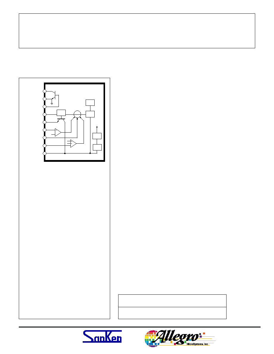
FUNCTIONAL BLOCK DIAGRAM
ALLOWABLE PACKAGE POWER DISSIPATION
MAXIMUM SAFE OPERATING AREA
PROPORTIONAL
DRIVE
TSD
OVER-VOLT.
PROTECT
OSC.
R
S
Q
V
IN
FDBK
OVER-CURRENT
PROTECTION
COMMON
COLLECTOR
BASE
SINK
DRIVE
3300 pF
1 k
0.7
Rton
Rtoff
0.75 V
-1 V
1.4 V
5.1 V
REF.
FAULT
LATCH
+
+
+
+
INHIBIT
9
8
5
4
3
1
2
6
7
Dwg. FK-001
UVLO
60
40
20
20
60
100
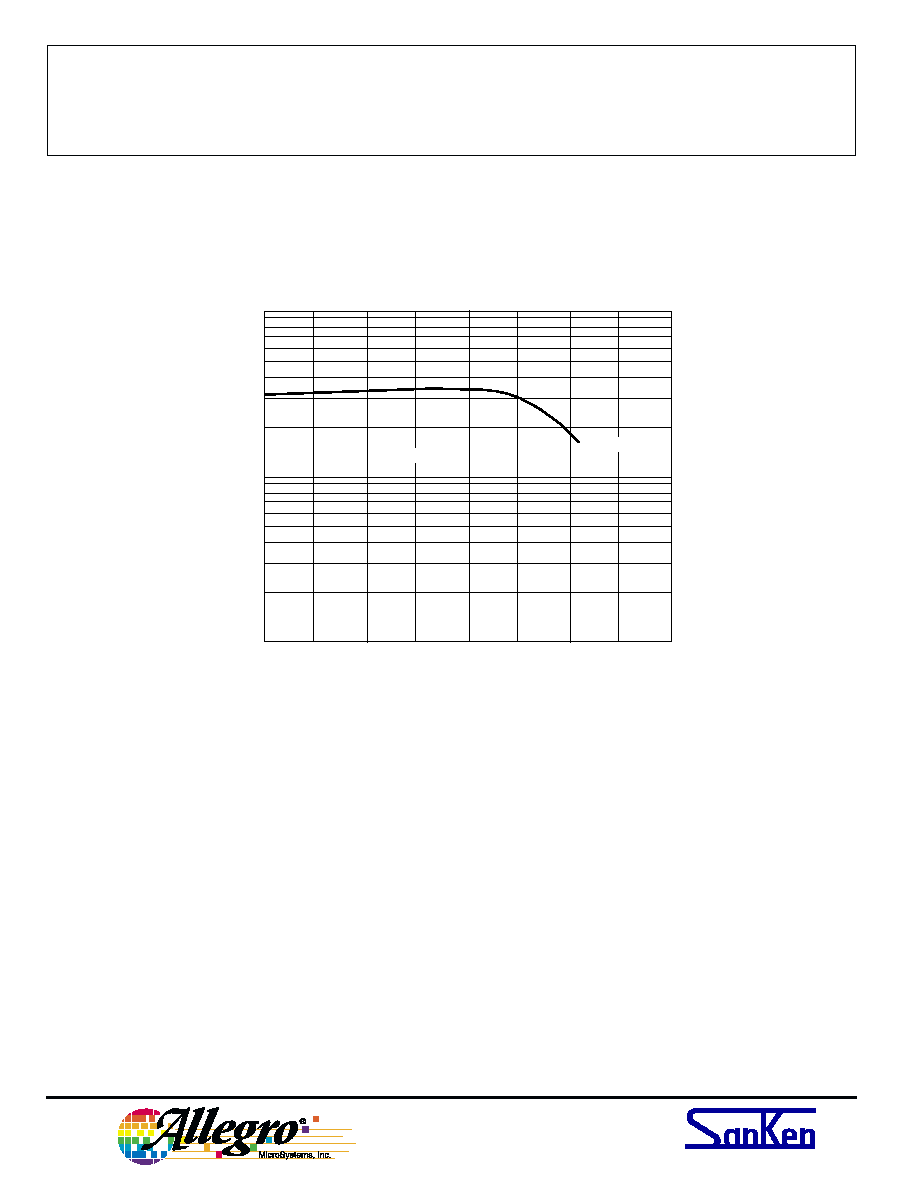
3.2 W
140
LIMITED BY FRAME
TEMP. = +125
∞C MAX.
RECOMMENDED MAX.
FRAME TEMP. = +100
∞C
FREE AIR
0
TEMPERATURE in
∞C
ALLOWABLE PACKAGE POWER DISSIPATION in WATTS
MOUNTING SURFACE
TEMPERATURE
Dwg. GK-003-3
STR-S6703 (54 W)
STR-S6704 (50 W)
30
3.0
0.3
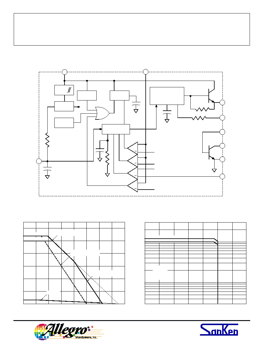
COLLECTOR-EMITTER VOLTAGE in VOLTS
COLLECTOR CURRENT in AMPERES
Dwg. GK-002-3
1.0
10
0
200
400
600
0.5
5.0
STR-S6704 (10 A)
STR-S6703 (12 A)
L = 6 mH
I
B1
= 2.5 A
I
B2
= 0.8 A
t
on
= 100
µs
dc < 1%
100
300
500
700
Copyright © 1994 Allegro MicroSystems, Inc.
STR-S6703
AND
STR-S6704
OFF-LINE
QUASI-RESONANT FLYBACK
SWITCHING REGULATORS
www.allegromicro.com
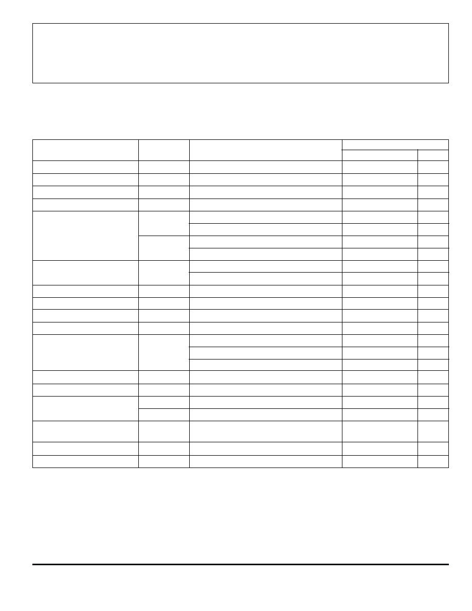
ELECTRICAL CHARACTERISTICS at T
A
= +25
∞
C, V
IN
= 8.5 V, voltage measurements are refer-
enced to Common (pin 2) (unless otherwise noted).
Limits
Characteristic
Symbol
Test Conditions
Min.
Typ. Max.
Units
On-State Voltage
V
INT
Turn-on, increasing V
IN
7.6
8.0
8.4
V
Under-Voltage Lockout
V
INQ
Turn-off, decreasing V
IN
4.6
4.9
5.2
V
Over-Voltage Threshold
V
OVP(th)
9.2
≠
10.7
V
Output Leakage Current
I
CEX
V
CE
= 500 V, V
BE
= -1.5 V
≠
≠
100
µA
Output Saturation Voltage
V
CE(sat)
STR-S6703, I
C
= 2 A, I
B
= 400 mA
≠
≠
400
mV
STR-S6704, I
C
= 2 A, I
B
= 400 mA
≠
≠
TBD
mV
V
BE(sat)
STR-S6703, I
C
= 2 A, I
B
= 400 mA
≠
≠
1.5
V
STR-S6704, I
C
= 2 A, I
B
= 400 mA
≠
≠
TBD
V
DC Current Gain
h
FE
STR-S6703, V
CE
= 4 V, I
C
= 1 A
23
≠
46
≠
STR-S6704, V
CE
= 4 V, I
C
= 1 A
20
≠
50
≠
Maximum ON Time
t
on
33
≠
41
µs
Minimum OFF Time
t
off
45
≠
55
µs
Over-Current Threshold
V
OCP(th)
-0.9
-1.0
-1.1
V
Feedback Threshold Volt.
V
FDBK(th)
≠
650
≠
mV
Inhibit Threshold Voltage
V
INH(th)
Oscillation stops
0.65
0.75
0.85
V
Oscillation synchronized
≠
1.4
2.0
V
Oscillation stops (fault latch set)
3.2
5.1
5.6
V
Latch Holding Current
I
INH
V
IN
reduced from 10.7 V to 4 V
≠
≠
500
µA
Latch Reset Voltage
V
Q
I
IN
100 µA, V
IN
reduced from 10.7 V
2.5
3.1
≠
V
Supply Current
I
IN(ON)
Operating
15
≠
28
mA
I
IN(OFF)
≠
≠
200
µA
Insulation RMS Voltage
V
WM(RMS)
All terminals simultaneous reference
2000
≠
≠
V
metal plate against backside
Thermal Shutdown
T
J
125
150
≠
∞C
Thermal Resistance
R
JM
Output junction to mounting surface
≠
2.0
≠
∞C/W
NOTES: Negative current is defined as coming out of (sourcing) the specified device terminal.
Typical Data is for design information only.
STR-S6703
AND
STR-S6704
OFF-LINE
QUASI-RESONANT FLYBACK
SWITCHING REGULATORS
www.allegromicro.com
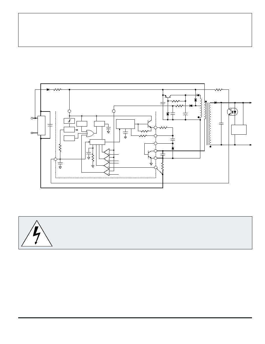
TYPICAL QUASI-RESONANT FLYBACK CONVERTER
WARNING: lethal potentials are present. See text.
APPLICATIONS INFORMATION
WARNING --
These devices are designed to be operated at lethal voltages and energy levels. Circuit
designs that embody these components must conform with applicable safety requirements. Precau-
tions must be taken to prevent accidental contact with power-line potentials. Do not connect
grounded test equipment.
The use of an isolation transformer is recommended during circuit development and breadboarding.
Recommended mounting hardware torque:
4.34 ≠ 5.79 lbf∑ft (6 ≠ 8 kg∑cm or 0.588 ≠ 0.784 Nm).
Recommended metal-oxide-filled, alkyl-degenerated oil base, silicone grease:
Dow Corning 340, or equivalent
+
VOLTAGE
SENSE
FULL-BRIDGE
RECTIFIER
AC INPUT
100 V/120 V
+ OUTPUT
≠ OUTPUT
+
+
Dwg. EK-004A
R
S
Q
+
+
+
+
9
8
5
4
3
1
2
7
6
+
+
#