 | –≠–ª–µ–∫—Ç—Ä–æ–Ω–Ω—ã–π –∫–æ–º–ø–æ–Ω–µ–Ω—Ç: STR-W6765 | –°–∫–∞—á–∞—Ç—å:  PDF PDF  ZIP ZIP |
STR-W6765
Description
The STR-W6765 is a quasi-resonant topology IC designed for
SMPS applications. It shows lower EMI noise characteristics
than conventional PWM solutions, especially at greater than
2 MHz. It also provides a soft-switching operation to turn on the
internal MOSFET at close to zero voltage (V
DS
bottom point)
by use of the resonant characteristic of primary inductance
and a resonant capacitor.
The package is a fully molded TO-220, which contains the
controller chip (MIC) and MOSFET, enabling output power up
to 52 W with universal input or 110 W with a 230 Vac input.
The bottom-skip function skips the first bottom of V
DS
and turns
on the MOSFET at the second bottom point, to minimize an
increase of operational frequency at light output load, improving
system-level efficiency over the entire load range.
There are two standby functions available to reduce the input
power under very light load conditions. The first is an auto-burst
mode operation that is internally triggered by periodic sensing,
and the other is a manual standby mode, which is executed
by clamping the secondary output. In general applications,
the manual standby mode reduces the input power further
compared to the auto-burst mode.
The soft-start function minimizes surge voltage and reduces
power stress to the MOSFET and to the secondary rectifying
Quasi-Resonant Topology
Primary Switching Regulators
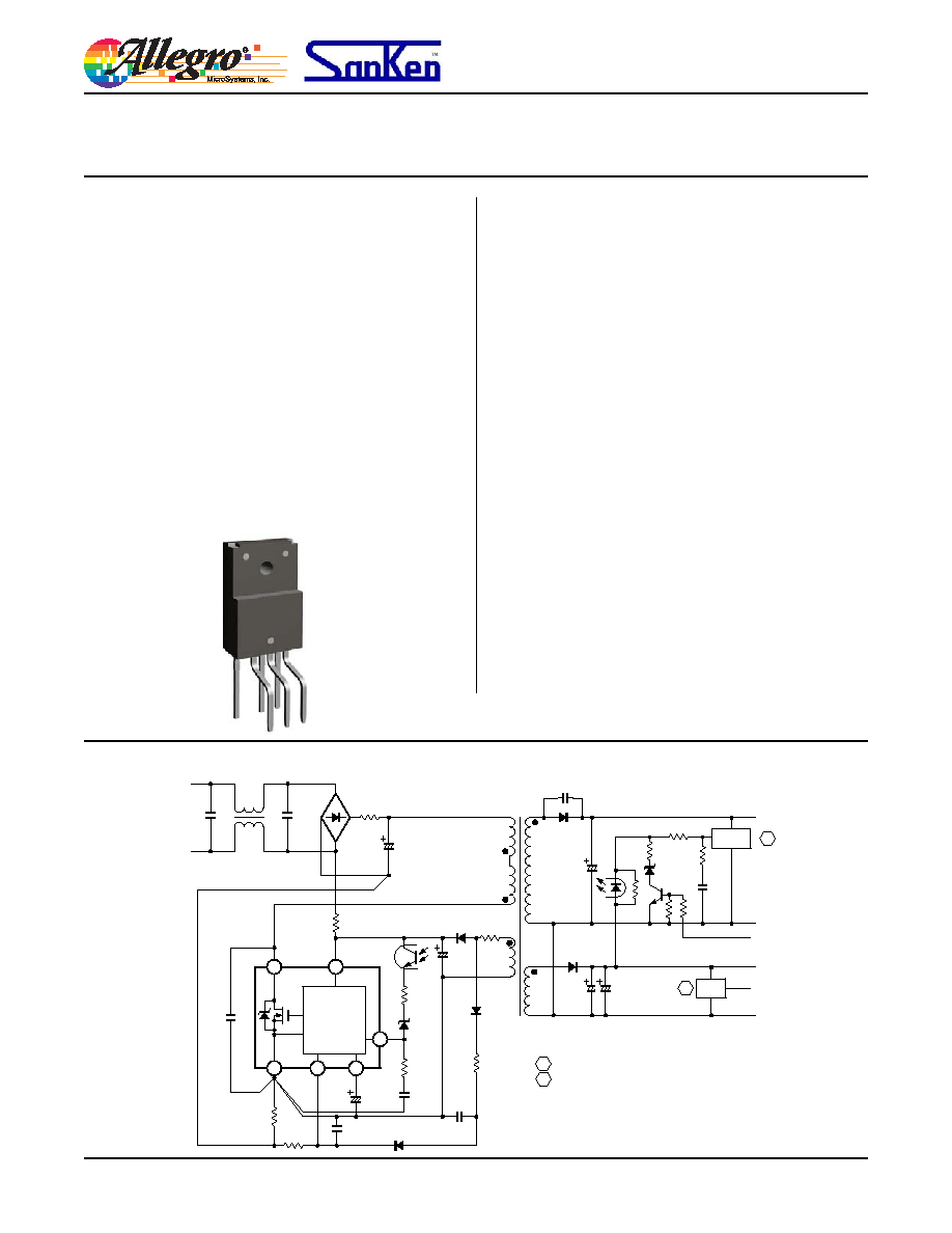
Typical Application
Package: 6-pin TO-220
Continued on the next page...
28103.30-6
Features and Benefits
Quasi-resonant topology IC
Low EMI noise and soft
switching
Bottom-skip
operation
Improved system efficiency
over the entire output load by avoiding increase of
switching frequency
Standby burst mode operation
Lowers input power at
very light output load condition
Avalanche-guaranteed
MOSFET
Improves system-
level reliability and does not require V
DSS
derating
800 V / 1.8 , 52 to 110 W (Universal/230 Vac input)
Continued on the next page...
+B
GND
S1
P
D
D
S/GND
V
CC
S2
LowB
GND
For ErrAmp, Sanken SE series device recommended
For SI, Sanken linear regulator IC recommended
1
1
3
3
7
7
Cont
STR-W6735
6
6
OCP
/BD
4
4
FB
ROCP
ErrAmp
SS
/OLP
5
5
Standby
ON/OFF
Standby
Out
CX
RX
SI
A
B
B
A
Quasi-Resonant Topology
Primary Switching Regulators
STR-W6765
2
Features and Benefits (continued)
Selection Guide
Part Number
Package
Packing
STR-W6765
TO-220
Bulk, 100 pieces
All performance characteristics given are typical values for circuit or
system baseline design only and are at the nominal operating voltage and
an ambient temperature of +25∞C, unless oth er wise stated.
Various
protections
Improved system-level reliability
Pulse-by-pulse drain overcurrent limiting
Overvoltage protection (bias winding voltage sensing),
with latch
Overload protection with latch
Maximum on-time limit
diodes during the start-up sequence. Various protections such as
overvoltage, overload, overcurrent, maximum on-time protections
and avalanche-energy-guaranteed MOSFET secure good system-
level reliability.
Applications include the following:
Set
Top
Box
LCD PC monitor, LCD TV
Printer,
Scanner
SMPS power supplies
Description (continued)
Absolute Maximum Ratings
at T
A
= 25∞C
Parameter
Symbol Terminal
Conditions
Rating
Unit
Drain Current
1
I
D
peak
1 - 3
Single pulse
11.2
A
Maximum Switching Current
2
I
Dmax
1 - 3
T
A
= ≠20∞C to 125∞C
11.2
A
Single Pulse Avalanche Energy
3
E
AS
1 - 3
Single pulse, V
DD
= 99 V, L = 20 mH,
I
Lpeak
= 5.8 A
300
mJ
Input Voltage for Controller (MIC)
V
CC
4 - 3
35
V
SS/OLP Terminal Voltage
V
SSOLP
5 - 3
≠0.5 to 6.0
V
FB Terminal Inflow Current
I
FB
6 - 3
10
mA
FB Terminal Voltage
V
FB
6 - 3
I
FB
within the limits of I
FB
≠0.5 to 9.0
V
OCP/BD Terminal Voltage
V
OCPBD
7 - 3
≠1.5 to 5.0
V
MOSFET Power Dissipation
4
P
D1
1 - 3
With infinite heatsink
28.7
W
Without heatsink
1.3
W
Controller (MIC) Power Dissipation
P
D2
4 - 3
V
CC
◊ I
CC
0.8
W
Operating Internal Leadframe Temperature
T
F
≠
Refer to T
OP
≠20 to 115
∞C
Operating Ambient Temperature
T
OP
≠
≠20 to 115
∞C
Storage Temperature
T
stg
≠
≠40 to 125
∞C
Junction Temperature
T
J
≠
150
∞C
1
Refer to figure 2
2
I
DMAX
is the drain current determined by the drive voltage of the IC and the threshold voltage, V
th
, of the MOSFET
3
Refer to figure 3
4
Refer to figure 5
Allegro MicroSystems, Inc.
115 Northeast Cutoff, Box 15036
Worcester, Massachusetts 01615-0036 (508) 853-5000
www.allegromicro.com
Quasi-Resonant Topology
Primary Switching Regulators
STR-W6765
3
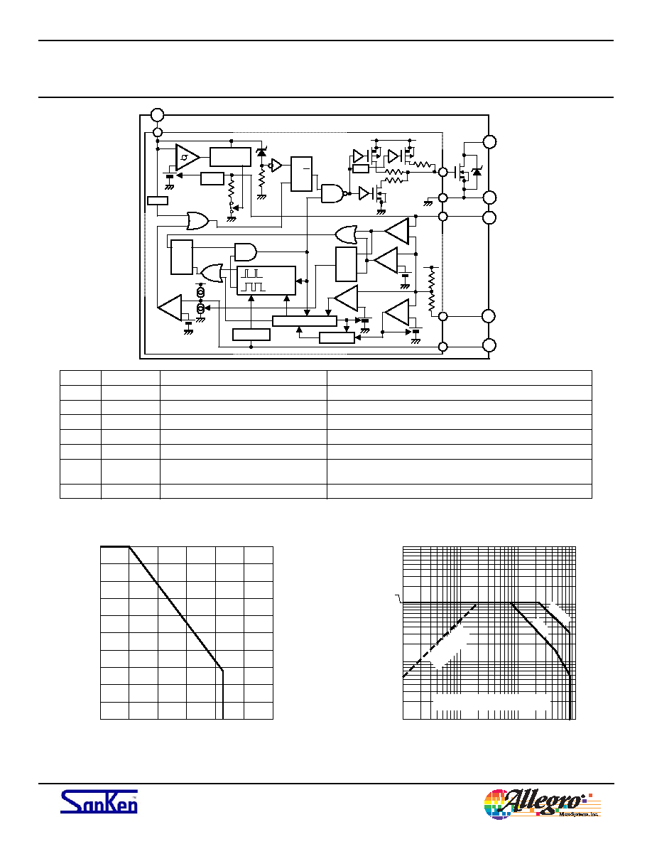
Temperature, T
F
(∞C)
Safe Operating Area
Temperature Derating Coef
ficient (%)
0
20
40
60
80
100
0
25
50
75
100
125
150
Drain-to-Source Voltage, V
DS
(V)
Drain Current, I
D
(A)
11.2
1.0
10.0
0.1
100.0
10
100
1000
1
1 ms
0.1 ms
Current limit
due to R
DS(on)
Refer to figure 1 for MOSFET SOA
temperature derating coefficient
Figure 1 ≠ MOSFET Safe Operating Area
Derating Curve
Figure 2 ≠ MOSFET Safe Operating Area
Drain Current versus Voltage
at T
A
= 25∞C, Single Pulse
D
S/GND
OCP/BD
V
CC
FB
Start
Stop
Burst
R
S
Q
Reg&
Iconst
OVP
DRIVE
Reg
Protection
latch
S
R Q
FB
OCP
BSD
BD
Bottom Selector
Counter
SS/OLP
OLP
Delay
S
R
Q
OSC
MaxON
Soft Start
Burst
Control
Burst
Control
4
+
-
+
-
+
-
+
-
+
-
+
-
1
3
6
7
5
Number
Name
Description
Functions
1
D
Drain
MOSFET drain
2
NC
Clipped
No connection
3
S/GND
Source/ground terminal
MOSFET source and ground
4
VCC
Power supply terminal
Input of power supply for control circuit
5
SS/OLP
Soft Start/Overload Protection terminal
Input to set delay for Overload Protection and Soft Start operation
6
FB
Feedback terminal
Input for Constant Voltage Control and Burst (intermittant)Mode
oscillation cotnrol signals
7
OCP/BD
Overcurrent Protection/Bottom Detection
Input for overcurrent detection and bottom detection signals
Allegro MicroSystems, Inc.
115 Northeast Cutoff, Box 15036
Worcester, Massachusetts 01615-0036 (508) 853-5000
www.allegromicro.com
Quasi-Resonant Topology
Primary Switching Regulators
STR-W6765
4
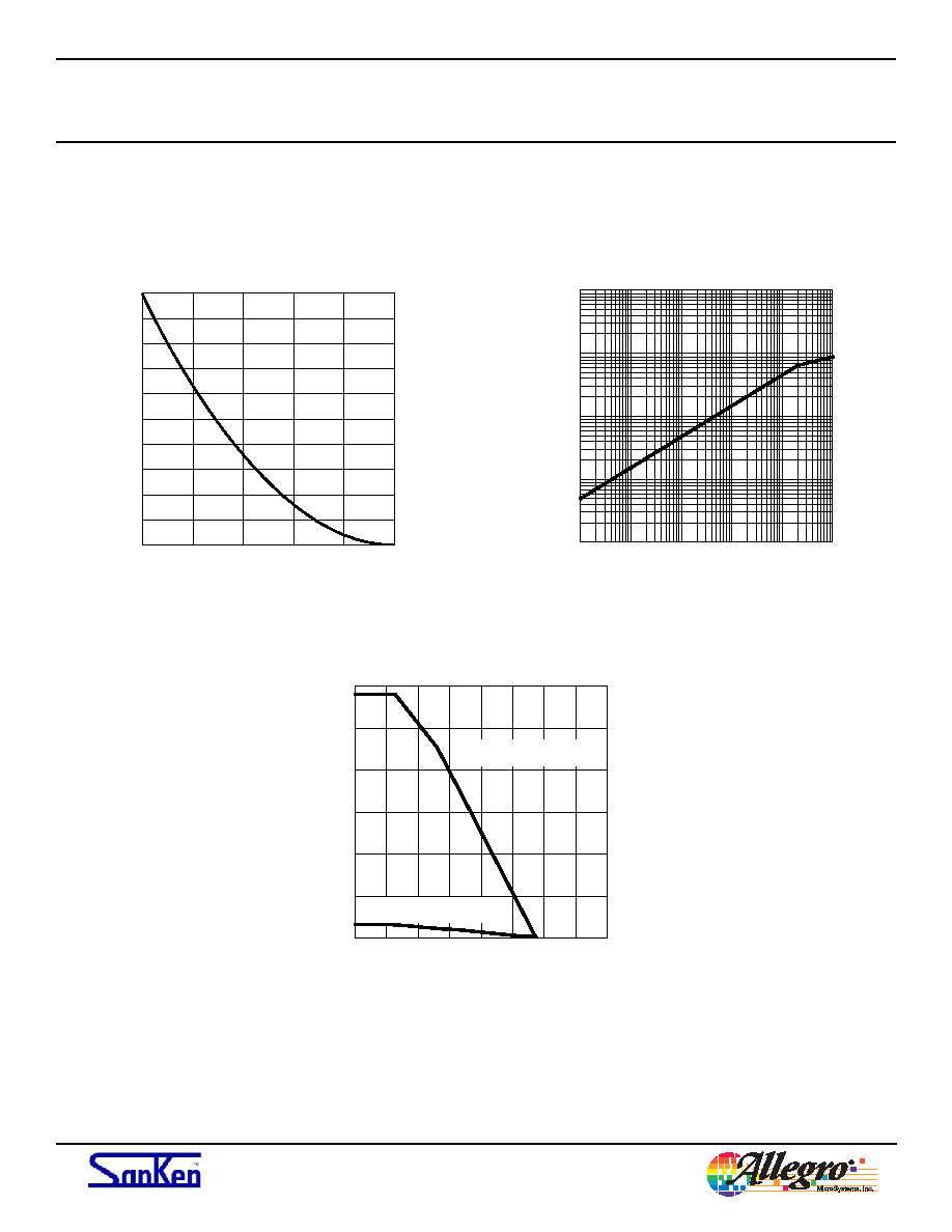
Channel Junction Temperature, T
J
(∞C)
E
AS
Temperature Derating Coef
ficient (%)
0
20
40
60
80
100
25
50
75
100
125
150
Time, t (s)
T
ransient
Thermal Resistance, R
JC
(∞C/W)
0.001
0.010
0.100
1.000
10.000
100
10
10m
1m
100m
1
Ambient Temperature, T
A
(∞C)
Power Dissipation, P
D1
(W)
0
5
10
15
20
25
30
0
20
40
60
80
100 120 140 160
P
D1
= 1.3 W at T
A
Without heatsink
With infinite heatsink
P
D1
= 28.7 W at T
A
Figure 3 ≠ MOSFET Avalanche Energy Derating Curve
Figure 4 ≠ Transient Thermal Resistance
Figure 5 ≠ MOSFET Power Dissipation versus Temperature
Allegro MicroSystems, Inc.
115 Northeast Cutoff, Box 15036
Worcester, Massachusetts 01615-0036 (508) 853-5000
www.allegromicro.com

Quasi-Resonant Topology
Primary Switching Regulators
STR-W6765
5
ELECTRICAL CHARACTERISTICS
Characteristic
Symbol
Terminals
Min.
Typ.
Max.
Units
ELECTRICAL CHARACTERISTICS for Controller (MIC)
1
, valid at T
A
= 25∞C, V
CC
= 20 V, unless otherwise specified
Power Supply Start-up Operation
Operation Start Voltage
V
CC(ON)
4 - 3
16.3
18.2
19.9
V
Operation Stop Voltage
V
CC(OFF)
4 - 3
8.8
9.7
10.6
V
Circuit Current In Operation
I
CC(ON)
4 - 3
≠
≠
6
mA
Circuit Current In Non-Operation
I
CC(OFF)
4 - 3
≠
≠
100
A
Oscillation Frequency
f
osc
1 - 3
19
22
25
kHz
Soft Start Operation Stop Voltage
V
SSOLP(SS)
5 - 3
1.1
1.2
1.4
V
Soft Start Operation Charging Current
I
SSOLP(SS)
5 - 3
≠710
≠550
≠390
A
Normal Operation
Bottom-Skip Operation Threshold Voltage 1
V
OCPBD(BS1)
7 - 3
≠0.720
≠0.665
≠0.605
V
Bottom-Skip Operation Threshold Voltage 2
V
OCPBD(BS2)
7 - 3
≠0.485
≠0.435
≠0.385
V
Overcurrent Detection Threshold Voltage
V
OCPBD(LIM)
7 - 3
≠0.995
≠0.940
≠0.895
V
OCP/BDOCP/BD Terminal Outflow Current
I
OCPBD
7 - 3
≠250
≠100
≠40
A
Quasi-Resonant Operation Threshold Voltage 1
V
OCPBD(TH1)
7 - 3
0.28
0.40
0.52
V
Quasi-Resonant Operation Threshold Voltage 2
V
OCPBD(TH2)
7 - 3
0.67
0.80
0.93
V
FB Terminal Threshold Voltage
V
FB(OFF)
6 - 3
1.32
1.45
1.58
V
FB Terminal Inflow Current (Normal Operation)
I
FB(ON)
6 - 3
600
1000
1400
A
Standby Operation
Standby Operation Start Voltage
V
CC(S)
4 - 3
10.3
11.1
12.1
V
Standby Operation Start Voltage Interval
V
CC(SK)
4 - 3
1.10
1.35
1.65
V
Standby Non-Operation Circuit Current
I
CC(S)
4 - 3
≠
20
56
A
FB Terminal Inflow Current, Standby Operation
I
FB(S)
6 - 3
≠
4
14
A
FB Terminal Threshold Voltage, Standby Operation
V
FB(S)
6 - 3
0.55
1.10
1.50
V
Minimum On Time
t
ON(MIN)
1 - 3
0.40
0.82
1.25
s
Maximum On Time
t
ON(MAX)
1 - 3
27.5
32.5
39.0
s
Protection Operation
Overload Protection Operation Threshold Voltage
V
SSOLP(OLP)
5 - 3
4.0
4.9
5.8
V
Overload Protection Operation Charging Current
I
SSOLP(OLP)
5 - 3
≠16
≠11
≠6
A
Overvoltage Protection Operation Voltage
V
CC(OVP)
4 - 3
25.5
27.7
29.9
V
Latch Circuit Holding Current
2
I
CC(H)
4 - 3
≠
45
140
A
Latch Circuit Release Voltage
2
V
CC(La.OFF)
4 - 3
6.0
7.2
8.5
V
ELECTRICAL CHARACTERISTICS for MOSFET
, valid at T
A
= 25∞C, unless otherwise specified
Drain-to-Source Breakdown Voltage
V
DSS
1 - 3
800
≠
≠
V
Drain Leakage Current
I
DSS
1 - 3
≠
≠
300
A
On Resistance
R
DS(on)
1 - 3
≠
≠
1.8
Switching Time
t
f
1 - 3
≠
≠
400
ns
Thermal Resistance
R
JA
Junction to Internal
Frame
≠
≠
1.55
∞C/W
1
Current polarity with respect to the IC: positive current indicates current sink at the terminal named, negative current indicates source at the
terminal named.
2
Latch circuit refers to operation during Overload Protection or Overvoltage Protection.
Allegro MicroSystems, Inc.
115 Northeast Cutoff, Box 15036
Worcester, Massachusetts 01615-0036 (508) 853-5000
www.allegromicro.com