 | –≠–ª–µ–∫—Ç—Ä–æ–Ω–Ω—ã–π –∫–æ–º–ø–æ–Ω–µ–Ω—Ç: UCN5833EP | –°–∫–∞—á–∞—Ç—å:  PDF PDF  ZIP ZIP |

Designed to reduce logic supply current, chip size, and system
cost, the UCN5833A/EP integrated circuits offer high-speed operation
for thermal printers. These devices can also be used to drive multi-
plexed LED displays or incandescent lamps within their 125 mA peak
output current rating. The combination of bipolar and MOS technolo-
gies gives BiMOS II smart power ICs an interface flexibility beyond the
reach of standard buffers and power driver circuits.
These 32-bit drivers have bipolar open-collector npn Darlington
outputs, a CMOS data latch for each of the drivers, a 32-bit CMOS
shift register, and CMOS control circuitry. The high-speed CMOS shift
registers and latches allow operation with most microprocessor-based
systems at data input rates above 3.3 MHz. Use of these drivers with
TTL may require input pull-up resistors to ensure an input logic high.
The UCN5833A is supplied in a 40-pin dual in-line plastic package
with 0.600" (15.24 mm) row spacing. At an ambient temperature of
+75
∞C, all outputs of the DlP-packaged device will sustain 50 mA
continuously. For high-density applications, the UCN5833EP is
available. This 44-lead plastic chip carrier (quad pack) is intended
for surface-mounting on solder lands with 0.050" (1.27 mm) centers.
CMOS serial data outputs permit cascading for applications requiring
additional drive lines.
FEATURES
I To 3.3 MHz Data Input Rate
I 30 V Minimum Output Breakdown
I Darlington Current-Sink Outputs
I Low-Power CMOS Logic and Latches
BiMOS II 32-BIT SERIAL-INPUT,
LATCHED DRIVER
UCN5833EP
ABSOLUTE MAXIMUM RATINGS
at +25
∞C Free-Air Temperature
Output Voltage, V
OUT
. . . . . . . . . . .
30 V
Logic Supply Voltage, V
DD
. . . . . . .
7.0 V
Input Voltage Range,
V
IN
. . . . . . . . .
-0.3 V to V
DD
+ 0.3 V
Continuous Output Current,
l
OUT
(each output) . . . . . . . . . . 125 mA
Package Power Dissipation, P
D
(UCN5833A) . . . . . . . . . . . . . . . 3.5 W*
(UCN5833EP) . . . . . . . . . . . . . . 2.5 W*
Operating Temperature Range,
T
A
. . . . . . . . . . . . . .
- 20
∞
C to +85
∞
C
Storage Temperature Range,
T
S
. . . . . . . . . . . . .
-55
∞
C to +150
∞
C
* Derate linearly to 0 W at +150
∞C.
Caution: CMOS devices have input static protection
but are susceptible to damage when exposed to
extremely high static electrical charges.
Always order by complete part number:
Part Number
Package
UCN5833A
40-Pin DIP
UCN5833EP
44-Lead PLCC
Dwg. No. A-13,049
1
4
5
6
18
19
20
21
22
23
24
25
26
27
28
40
41
42
43
44
2
3
7
8
9
10
11
12
13
14
15
16
17
OUT
2
OUT
3
OUT
4
OUT
5
OUT
6
OUT
7
OUT
8
OUT
9
OUT
OUT
10
OUT
11
12
OUT
NC
STROBE
1
POWER GROUND
SERIAL
DA
T
A
IN
LOGIC
SUPPL
Y
CLOCK
SERIAL
DA
T
A
OUT
OUTPUT
ENABLE
NC
OUT
32
38
39
37
36
35
34
33
32
31
30
29
OUT
31
OUT
30
OUT
29
OUT
28
OUT
27
OUT
26
OUT
25
OUT
24
OUT
23
OUT
22
OUT
21
NC
OUT
13
OUT
14
OUT
15
OUT
16
LOGIC GROUND
OUT
17
OUT
18
OUT
19
OUT
20
NC
SUB
REGISTER
REGISTER
LA
TCHES
LA
TCHES
ST
CLK
OE
V
DD
Data Sheet
26185.16A*
5833

5833
BiMOS II 32-BIT
SERIAL-INPUT,
LATCHED DRIVER
115 Northeast Cutoff, Box 15036
Worcester, Massachusetts 01615-0036 (508) 853-5000
V
CLK
DD
SERIAL
DATA IN
POWER
GROUND
STROBE
OUT
OUT
OUT
OUT
OUT
OUT
1
2
3
4
5
6
OUT
7
OUT
8
OUT
9
OUT
10
OUT
11
OUT
12
OUT
13
OUT
14
OUT
18
OUT
19
OUT
20
OUT
21
OUT
22
OUT
23
OUT
24
OUT
25
OUT
26
OUT
27
OUT
28
OUT
29
OUT
30
OUT
31
OUT
32
OUTPUT
ENABLE
LOGIC
SUPPLY
SERIAL
DATA OUT
LOGIC
GROUND
SUB
LOGIC
SUPPLY
40
39
38
37
34
35
36
31
32
33
30
22
29
28
27
26
25
24
23
21
1
2
3
4
7
6
5
10
9
8
11
12
12
14
15
16
17
18
19
20
ST
OUT
15
OUT
16
OUT
17
LA
TCHES
REGISTER
REGISTER
LA
TCHES
OE
Dwg. No. A-13,057
TYPICAL INPUT CIRCUIT
FUNCTIONAL BLOCK DIAGRAM
Dwg. No. A-13,048
Dwg. No. A-13,051
Dwg. No. A-13,050
TYPICAL OUTPUT DRIVER
UCN5833A
32-BIT SHIFT REGISTER
LATCHES
CLOCK
SERIAL
DATA IN
STROBE
OUTPUT
ENABLE
LOGIC
GROUND
V
DD
SERIAL DATA
OUT
SUB
MOS
BIPOLAR
OUT
OUT OUT
OUT
OUT
OUT
1
2
3
30
31
32
POWER
GROUND
IN
SUB
V
DD
OUT
115 Northeast Cutoff, Box 15036
Worcester, Massachusetts 01615-0036 (508) 853-5000
Copyright © 1986, 1995, Allegro MicroSystems, Inc.
CLOCK
5833
BiMOS II 32-BIT
SERIAL-INPUT,
LATCHED DRIVER
TRUTH TABLE
Serial
Shift Register Contents
Serial
Latch Contents
Output Output Contents
Data
Clock
Data
Strobe
Enable
Input
Input I
1
I
2
I
3
...
I
N-1
I
N
Output
Input
I
1
I
2
I
3
...
I
N-1
I
N
Input
I
1
I
2
I
3
... I
N-1
I
N
H
H
R
1
R
2
...
R
N-2
R
N-1
R
N-1
L
L
R
1
R
2
...
R
N-2
R
N-1
R
N-1
X
R
1
R
2
R
3
...
R
N-1
R
N
R
N
X
X
X
...
X
X
X
L
R
1
R
2
R
3
...
R
N-1
R
N
P
1
P
2
P
3
...
P
N-1
P
N
P
N
H
P
1
P
2
P
3
...
P
N-1
P
N
H
P
1
P
2
P
3
... P
N-1
P
N
X
X
X
...
X
X
L
H
H
H
... H H
L = Low Logic Level H = High Logic Level X = Irrelevant P = Present State R = Previous State
ELECTRICAL CHARACTERISTICS at T
A
= +25
∞
C, V
DD
= 5 V (unless otherwise noted).
Limits
Characteristic
Symbol
Test Conditions
Min.
Max.
Units
Output Leakage Current
I
CEX
V
OUT
= 30 V, T
A
= 70
∞C
--
10
µA
Collector-Emitter
V
CE(SAT)
l
OUT
= 50 mA
--
1.2
V
l
OUT
= 100 mA
--
1.7
V
Input Voltage
V
IN(1)
3.5
5.3
V
V
IN(0)
-0.3
+0.8
V
Input Current
l
IN(1)
V
IN
= 5.0 V
--
1.0
µA
l
IN(0)
V
IN
= 0 V
--
-1.0
µA
Serial Output Voltage
V
OUT(1)
I
OUT
= -200
µA
4.5
--
V
V
OUT(0)
I
OUT
= 200
µA
--
0.3
V
Supply Current
l
DD
One output ON, l
OUT
= 100 mA
--
1.0
mA
All outputs OFF
--
50
µA
Output Rise Time
t
r
l
OUT
= 100 mA, 10% to 90%
--
500
ns
Output Fall Time
t
f
l
OUT
= 100 mA, 90% to 10%
--
500
ns
NOTE: Positive (negative) current is defined as going into (coming out of) the specified device pin.
Saturation Voltage
5833
BiMOS II 32-BIT
SERIAL-INPUT,
LATCHED DRIVER
115 Northeast Cutoff, Box 15036
Worcester, Massachusetts 01615-0036 (508) 853-5000
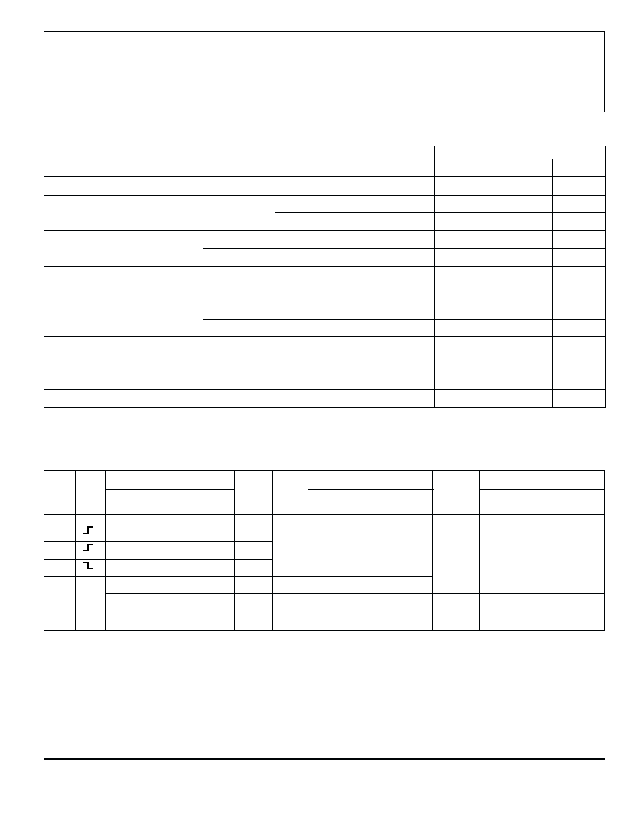
TIMING CONDITIONS
(V
DD
= 5.0 V, Logic Levels are V
DD
and Ground)
A. Minimum Data Active Time Before Clock Pulse
(Data Set-Up Time) .......................................................................... 75 ns
B. Minimum Data Active Time After Clock Pulse
(Data Hold Time) ............................................................................. 75 ns
C. Minimum Data Pulse Width ................................................................ 150 ns
D. Minimum Clock Pulse Width ............................................................... 150 ns
E. Minimum Time Between Clock Activation and Strobe ....................... 300 ns
F. Minimum Strobe Pulse Width ............................................................. 100 ns
G. Typical Time Between Strobe Activation and
Output Transition ........................................................................... 500 ns
Dwg. No. A-12,276A
Serial Data present at the input is transferred to the shift register
on the logic "0" to logic "1" transition of the CLOCK input pulse. On
succeeding CLOCK pulses, the registers shift data information towards
the SERIAL DATA OUTPUT. The SERIAL DATA must appear at the
input prior to the rising edge of the CLOCK input waveform.
Information present at any register is transferred to its respective
latch when the STROBE is high (serial-to-parallel conversion). The
latches will continue to accept new data as long as the STROBE is
held high. Applications where the latches are bypassed (STROBE tied
high) will require that the OUTPUT ENABLE input be low during serial
data entry.
When the OUTPUT ENABLE input is low, all of the output buffers
are disabled (OFF) without affecting the information stored in the
latches or shift register. With the OUTPUT ENABLE input high, the
outputs are controlled by the state of the latches.
E F
CLOCK
DATA IN
STROBE
N
A D
B
C
G
OUTPUT
ENABLE
OUT
5833
BiMOS II 32-BIT
SERIAL-INPUT,
LATCHED DRIVER
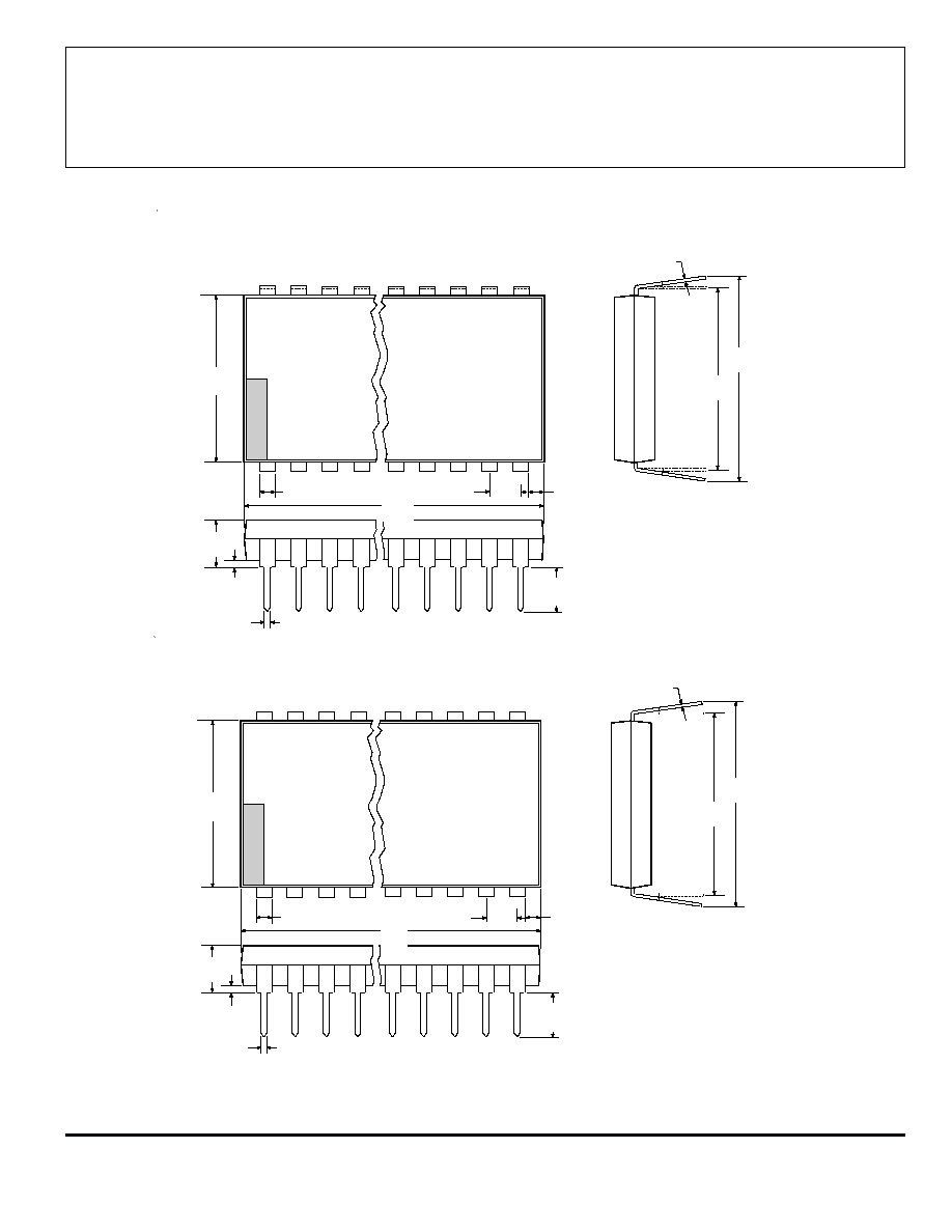
NOTES: 1. Exact body and lead configuration at vendor's option within limits shown.
2. Lead spacing tolerance is non-cumulative.
3. Lead thickness is measured at seating plane or below.
UCN5833A
Dimensions in Inches
(controlling dimensions)
Dimensions in Millimeters
(for reference only)
40
14.73
12.32
1
2
3
6.35
MAX
1.77
0.77
0.39
MIN
0.558
0.356
0.381
0.204
15.24
BSC
Dwg. MA-003-40 mm
20
2.54
BSC
0.13
MIN
5.08
2.93
4
17.78
MAX
21
53.2
50.3
40
0.580
0.485
1
2
3
0.250
MAX
0.070
0.030
0.015
MIN
0.022
0.014
0.015
0.008
0.600
BSC
Dwg. MA-003-40 in
20
0.100
BSC
0.005
MIN
0.200
0.115
4
0.700
MAX
21
2.095
1.980