Frequently applied in non-impact printer systems, the UCN5890A,
UCN5890LW, UCN5891A, and UCN5891LW are BiMOS II serial-input,
latched source (high-side) drivers. The octal, high-current smart-power ICs
merge an 8-bit CMOS shift register, associated CMOS latches, and CMOS
control logic (strobe and output enable) with sourcing power Darlington
outputs. Typical applications include multiplexed LED and incandescent
displays, relays, solenoids, and similar peripheral loads to a maximum of
-500 mA per output.
Except for output voltage ratings, these smart high-side driver ICs are
equivalent. The UCN5890A/LW are rated for operation with load supply
voltages of 20 V to 80 V and a minimum output sustaining voltage of 50 V.
The UCN5891A/LW are optimized for operation with supply voltages of 5 V
to 50 V (35 V sustaining).
BiMOS II devices have higher data-input rates than the original BiMOS
circuits. With a 5 V supply, they will operate to at least 3.3 MHz. At 12 V,
higher speeds are possible. The CMOS inputs are compatible with standard
CMOS and NMOS logic levels. TTL circuits may require the use of appropri-
ate pull-up resistors to ensure a proper input-logic high. A CMOS serial data
output, allows cascading these devices in multiple drive-line applications
required by many dot matrix, alphanumeric, and bar graph displays.
Suffix `A' devices are supplied in a standard dual in-line plastic package
with copper lead frame for enhanced package power dissipation characteris-
tics. Suffix `LW' devices are supplied in a standard wide-body SOIC package
for surface-mount applications. Similar driver, featuring reduced output
saturation voltage, are the UCN5895A and A5895SLW. Complementary,
8-bit serial-input, latched sink drivers are the Series UCN5820A.
FEATURES
I 50 V or 80 V Source Outputs
I Output Current to -500 mA
I Output Transient-Suppression Diodes
I To 3.3 MHz Data-lnput Rate
I Low-Power CMOS Logic and Latches
BIMOS II 8-BIT SERIAL-INPUT,
LATCHED SOURCE DRIVERS
Data Sheet
26182.12C
ABSOLUTE MAXIMUM RATINGS
at T
A
= +25
�C
Output Voltage, V
OUT
(UCN5890A & UCN5890LW) ......... 80 V
(UCN5891A & UCN5891LW) ......... 50 V
Logic Supply Voltage Range,
V
DD
.................................... 4.5 V to 15 V
Driver Supply Voltage Range, V
BB
(UCN5890A/LW) ................ 20 V to 80 V
(UCN5891A/LW) ............... 5.0 V to 50 V
Input Voltage Range,
V
IN
........................ -0.3 V to V
DD
+ 0.3 V
Continuous Output Current,
I
OUT
........................................... -500 mA
Allowable Package Power Dissipation,
P
D
......................................... See Graph
Operating Temperature Range,
T
A
.................................. -20
�
C to +85
�
C
Storage Temperature Range,
T
S
................................ -55
�
C to +150
�
C
Caution: CMOS devices have input static
protection, but are susceptible to damage when
exposed to extremely high static electrical
charges.
Always order by complete part number, e.g., UCN5891LW .
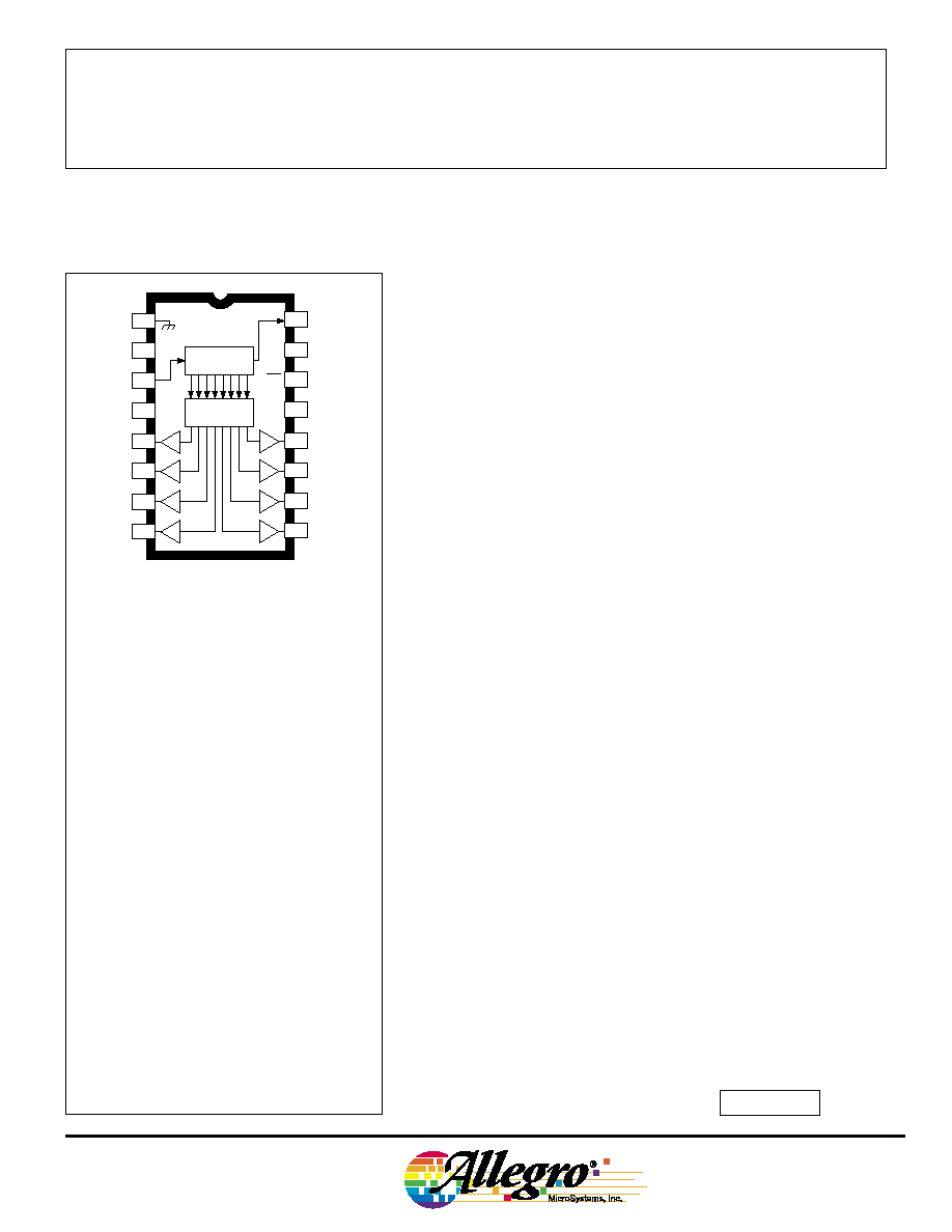
5890
AND
5891
Note the suffix `A' devices (DIP) and the suffix
`LW' devices (SOIC) are electrically identical and
share a common terminal number assignment.
2
3
4
5
6
7
8
SERIAL
DATA OUT
SERIAL
DATA IN
OUTPUT
ENABLE
LOGIC
SUPPLY
STROBE
CLOCK
CLK
V
DD
ST
OE
1
GROUND
9
10
11
12
13
14
15
16
OUT
1
OUT
2
OUT
3
Dwg. PP-026-2A
OUT
5
OUT
6
OUT
7
OUT
8
OUT
4
SHIFT
REGISTER
LATCHES
V
BB
LOAD
SUPPLY
5890
AND
5891
8-BIT SERIAL-INPUT,
LATCHED SOURCE DRIVERS
115 Northeast Cutoff, Box 15036
Worcester, Massachusetts 01615-0036 (508) 853-5000
Dwg. No. A-12,654
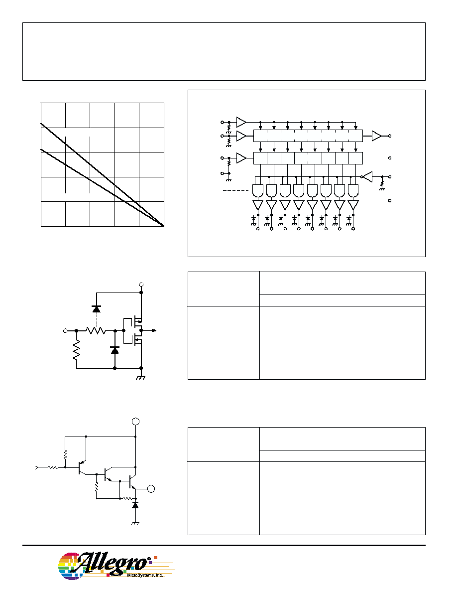
FUNCTIONAL BLOCK DIAGRAM
8-BIT SERIAL-PARALLEL SHIFT REGISTER
GROUND
STROBE
SERIAL
DATA IN
CLOCK
LATCHES
MOS
BIPOLAR
VBB
SERIAL
DATA OUT
VDD
OUTPUT
ENABLE
OUT1 OUT2 OUT3 OUT4 OUT5 OUT6 OUT7 OUT8
Number of
UCN5890/91A Max. Allowable Duty Cycle
Outputs On at
at T
A
of
I
OUT
= -200 mA
50
�
C
60
�
C
70
�
C
8
53%
47%
41%
7
60%
54%
48%
6
70%
64%
56%
5
83%
75%
67%
4
100%
94%
84%
3
100%
100%
100%
2
100%
100%
100%
1
100%
100%
100%
Copyright � 1985, 2000 Allegro MicroSystems, Inc.
50
75
100
125
150
2.5
0.5
0
AMBIENT TEMPERATURE IN
�C
2.0
1.5
1.0
25
Dwg. GP-018B
SUFFIX 'A', R = 60
�C/W
JA
SUFFIX 'LW', R = 80
�C/W
JA
ALLOWABLE PACKAGE POWER DISSIPATION IN WATTS
Dwg. EP-010-4A
IN
V
DD
TYPICAL INPUT CIRCUIT
Dwg. No. A-12,648
V
BB
OUT
TYPICAL OUTPUT DRIVER
Number of
UCN5890/91LW Max. Allowable Duty Cycle
Outputs On at
at T
A
of
I
OUT
= -200 mA
50
�
C
60
�
C
70
�
C
8
40%
35%
31%
7
45%
41%
36%
6
53%
48%
42%
5
62%
56%
50%
4
80%
71%
62%
3
100%
96%
84%
2
100%
100%
100%
1
100%
100%
100%
5890
AND
5891
8-BIT SERIAL-INPUT,
LATCHED SOURCE DRIVERS
www.allegromicro.com
ELECTRICAL CHARACTERISTICS at T
A
= +25
�
C, V
BB
= 80 V (UCN5890A/LW) or 50 V
(UCN5891A/LW), V
DD
= 5 V and 12 V (unless otherwise noted).
Limits
Characteristic
Symbol
V
BB
Test Conditions
Min.
Max.
Units
Output Leakage Current
I
CEX
Max.
T
A
= +25
�C
--
-50
�A
T
A
= +70
�C
--
-100
�A
Output Saturation Voltage
V
CE(SAT)
50 V
I
OUT
= -100 mA
--
1.8
V
I
OUT
= -225 mA
--
1.9
V
I
OUT
= -350 mA
--
2.0
V
Output Sustaining Voltage
V
CE(sus)
Max.
I
OUT
= -350 mA, L = 2 mH, UCN5891A/LW
35
--
V
I
OUT
= -350 mA, L = 2 mH, UCN5890A/LW
50
--
V
Input Voltage
V
IN(1)
50 V
V
DD
= 5.0 V
3.5
5.3
V
V
DD
= 12 V
10.5
12.3
V
V
IN(0)
50 V
V
DD
= 5 V to 12 V
-0.3
+0.8
V
Input Current
I
IN(1)
50 V
V
DD
= V
IN
= 5.0 V
--
50
�A
V
DD
= V
IN
= 12 V
--
240
�A
Input lmpedance
Z
IN
50 V
V
DD
= 5.0 V
100
--
k
V
DD
= 12 V
50
--
k
Max. Clock Frequency
f
c
50 V
3.3*
--
MHz
Serial Data Output
R
OUT
50 V
V
DD
= 5.0 V
--
20
k
Resistance
V
DD
= 12 V
--
6.0
k
Turn-On Delay
t
PLH
50 V
Output Enable to Output, I
OUT
= -350 mA
--
2.0
�s
Turn-Off Delay
t
PHL
50 V
Output Enable to Output, I
OUT
= -350 mA
--
10
�s
Supply Current
I
BB
50 V
All outputs on, All outputs open
--
10
mA
All outputs off
--
200
�A
l
DD
50 V
V
DD
= 5 V, All outputs off, Inputs = 0 V
--
100
�A
V
DD
= 12 V, All outputs off, Inputs = 0 V
--
200
�A
V
DD
= 5 V, One output on, All Inputs = 0 V
--
1.0
mA
V
DD
= 12 V, One output on, All Inputs = 0 V
--
3.0
mA
Diode Leakage Current
I
R
Max.
T
A
= +25
�C
--
50
�A
T
A
= +70
�C
--
100
�A
Diode Forward Voltage
V
F
Open
I
F
= 350 mA
--
2.0
V
NOTES: Turn-off delay is influenced by load conditions. Systems applications well below the specified output loading may require
timing considerations for some designs, i.e., multiplexed displays or when used in combination with sink drivers in a totem
pole configuration.
Positive (negative) current is defined as going into (coming out of) the specified device pin.
* Operation at a clock frequency greater than the specified minimum value is possible but not warranteed.

5890
AND
5891
8-BIT SERIAL-INPUT,
LATCHED SOURCE DRIVERS
115 Northeast Cutoff, Box 15036
Worcester, Massachusetts 01615-0036 (508) 853-5000
Serial
Shift Register Contents
Serial
Latch Contents
Output Contents
Data
Clock
Data
Strobe
Output
Input
Input I
1
I
2
I
3
...
I
N-1
I
N
Output
Input
I
1
I
2
I
3
...
I
N-1
I
N
Enable
I
1
I
2
I
3
... I
N-1
I
N
H
H
R
1
R
2
...
R
N-2
R
N-1
R
N-1
L
L
R
1
R
2
...
R
N-2
R
N-1
R
N-1
X
R
1
R
2
R
3
...
R
N-1
R
N
R
N
X
X
X
...
X
X
X
L
R
1
R
2
R
3
...
R
N-1
R
N
P
1
P
2
P
3
...
P
N-1
P
N
P
N
H
P
1
P
2
P
3
...
P
N-1
P
N
L
P
1
P
2
P
3
... P
N-1
P
N
X
X
X
...
X
X
H
L
L
L
... L
L
E F
CLOCK
DATA IN
STROBE
BLANKING
OUT
N
A D
B
C
G
Serial Data present at the input is transferred
to the shift register on the logic "0" to logic "1"
transition of the CLOCK input pulse. On
succeeding CLOCK pulses, the registers shift data
information towards the SERIAL DATA OUT-
PUT. The SERIAL DATA must appear at the
input prior to the rising edge of the CLOCK input
waveform.
Information present at any register is trans-
ferred to the respective latch when the STROBE
is high (serial-to-parallel conversion). The
latches will continue to accept new data as long as
the STROBE is held high. Applications where
the latches are bypassed (STROBE tied high) will
require that the OUTPUT ENABLE input be high
during serial data entry.
When the OUTPUT ENABLE input is high,
all of the output buffers are disabled (off) without
affecting the information stored in the latches or
shift register. With the OUTPUT ENABLE input
low, the outputs are controlled by the state of
their respective latches.
Dwg. No. A-12,649A
TIMING REQUIREMENTS
(T
A
= +25
�C,V
DD
= 5 V, Logic Levels are V
DD
and Ground)
A. Minimum Data Active Time Before Clock Pulse
(Data Set-Up Time) .......................................................................... 75 ns
B. Minimum Data Active Time After Clock Pulse
(Data Hold Time) ............................................................................. 75 ns
C. Minimum Data Pulse Width ................................................................ 150 ns
D. Minimum Clock Pulse Width ............................................................... 150 ns
E. Minimum Time Between Clock Activation and Strobe ....................... 300 ns
F. Minimum Strobe Pulse Width ............................................................. 100 ns
G. Typical Time Between Strobe Activation and
Output Transistion ......................................................................... 500 ns
Timing is representative of a 3.3 MHz clock. Higher speeds may be attainable
with increased supply voltage; operation at high temperatures will reduce the
specified maximum clock frequency.
TRUTH TABLE
L = Low Logic Level H = High Logic Level X = Irrelevant P = Present State R = Previous State

5890
AND
5891
8-BIT SERIAL-INPUT,
LATCHED SOURCE DRIVERS
www.allegromicro.com
TYPICAL APPLICATION
SOLENOID OR RELAY DRIVER
OUTPUT ENABLE
8
7
6
3
2
1
5
4
OE
DD
V
SHIFT
REGISTER
BB
V
LATCHES
DATA OUT
(ACTIVE LOW)
+5V +48V
16
15
14
11
10
9
13
12
CLOCK
DATA IN
STROBE
UCN5890A
Dwg. No. A-12,548
The products described here are manufactured under one or more
U.S. patents or U.S. patents pending.
Allegro MicroSystems, Inc. reserves the right to make, from time to
time, such departures from the detail specifications as may be
required to permit improvements in the performance, reliability, or
manufacturability of its products. Before placing an order, the user is
cautioned to verify that the information being relied upon is current.
Allegro products are not authorized for use as critical components
in life-support devices or systems without express written approval.
The information included herein is believed to be accurate and
reliable. However, Allegro MicroSystems, Inc. assumes no responsi-
bility for its use; nor for any infringement of patents or other rights of
third parties which may result from its use.