BiMOS II 10-BIT SERIAL-INPUT, LATCHED
SOURCE DRIVERS WITH ACTIVE-DMOS PULL-DOWNS
Always order by complete part number, e.g., UCN5810AF .
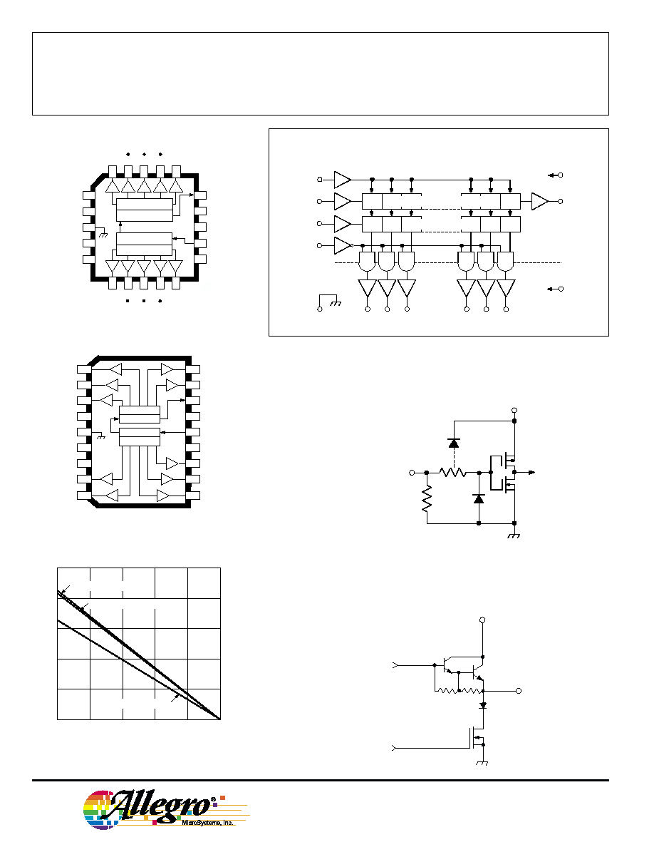
The UCN5810AF, UCN5810EPF, and UCN5810LWF combine a 10-bit
CMOS shift register and accompanying data latches, control circuitry, bipolar
sourcing outputs with DMOS active pull-downs. Designed primarily to drive
vacuum-fluorescent displays, the 60 V and -40 mA output ratings also allow
these devices to be used in many other peripheral power driver applications.
The UCN5810AF/EPF/LWF feature reduced supply requirements (active
DMOS pull-downs) and lower saturation voltages when compared with the
original UCN5810A.
The CMOS shift register and latches allow direct interfacing with
microprocessor-based systems. With a 5 V supply, they will operate to at
least 3.3 MHz. At 12 V, higher speeds are possible. Use with TTL may
require appropriate pull-up resistors to ensure an input logic high.
A CMOS serial data output enables cascade connections in applications
requiring additional drive lines. Similar devices are available as the
UCN5811A (12 bits), UCN5812AF/EPF (20 bits), and UCN5818AF/EPF (32
bits).
The UCN5810AF/EPF/LWF output source drivers are NPN Darlingtons
capable of sourcing up to 40 mA. The DMOS active pull-downs are capable
of sinking up to 15 mA. For inter-digit blanking, all of the output drivers can
be disabled and the DMOS sink drivers turned on by the BLANKING input
high.
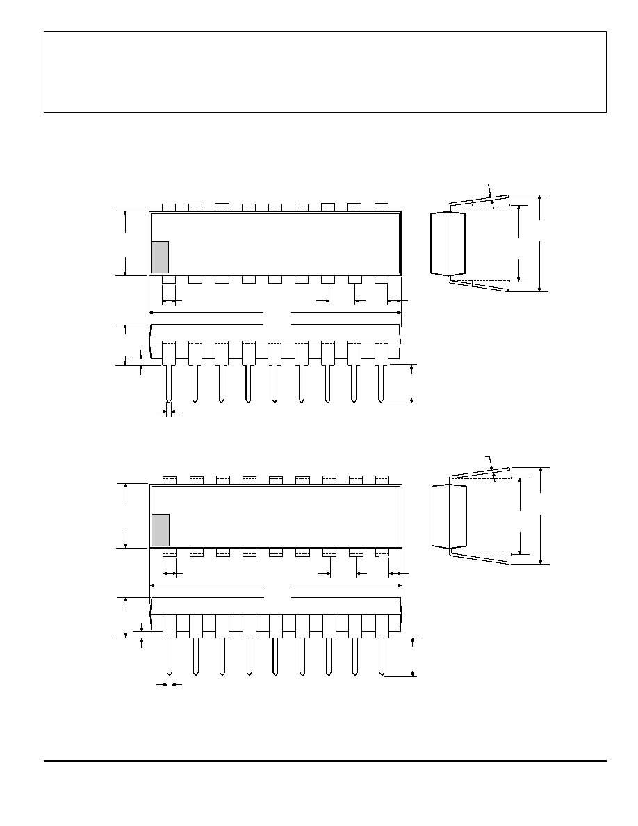
The UCN5810AF is furnished in an 18-pin dual in-line plastic package.
The UCN5810EPF is furnished in a 20-lead plastic chip carrier. The
UCN5810LWF is furnished in a wide-body, small-outline plastic package
(SOIC) with gull-wing leads. Copper lead frames, reduced supply current
requirements, and lower output saturation voltages allow all devices to source
25 mA from all outputs continuously, over the entire operating temperature
range. All devices are also available for operation between -40
�C and +85�C.
To order, change the prefix from `UCN' to `UCQ'.
FEATURES
I High-Speed Source Drivers
I 60 V Minimum
Output Breakdown
I Improved Replacements
for TL4810B
UCN5810AF
Data Sheet
26182.24C
2
3
4
5
6
7
8
9
10
11
12
13
14
15
16
17
18
SERIAL
DATA OUT
LOAD
SUPPLY
SERIAL
DATA IN
BLANKING
LOGIC
SUPPLY
STROBE
GROUND
CLOCK
CLK
V
ST
BLNK
DD
BB
V
OUT
9
OUT
10
OUT
1
OUT
2
OUT
3
Dwg. PP-029
OUT
8
OUT
7
OUT
6
OUT
5
OUT
4
1
LATCHES
REGISTER
REGISTER
LATCHES
ABSOLUTE MAXIMUM RATINGS
at T
A
= 25
�C
Logic Supply Voltage, V
DD
..................... 15 V
Driver Supply Voltage, V
BB
.................... 60 V
Continuous Output Current Range,
I
OUT
.......................... -40 mA to +15 mA
Input Voltage Range,
V
IN
........................ -0.3 V to V
DD
+ 0.3 V
Package Power Dissipation, P
D
(UCN5810AF) ........................... 2.27 W*
(UCN5810EPF) ........................ 1.78 W*
(UCN5810LWF) ........................ 1.56 W*
Operating Temperature Range,
T
A
.................................. -20
�
C to +85
�
C
Storage Temperature Range,
T
S
................................ -55
�
C to +150
�
C
*Derate linearly to 0 W at +150
�C.
Caution: CMOS devices have input static
protection but are susceptible to damage when
exposed to extremely high static electrical
charges.
Note that the UCN5810AF (dual in-line package)
and UCN5810LWF (small-outline IC package) are
electrically identical and share a common pin
number assignment.
I Low Output Saturation Voltages
I Low-Power CMOS Logic
and Latches
I To 3.3 MHz Data Input Rate
I Active DMOS Pull-Downs
5810-F

5810-F
10-BIT SERIAL-INPUT,
LATCHED SOURCE DRIVERS
WITH ACTIVE-DMOS PULL-DOWNS
115 Northeast Cutoff, Box 15036
Worcester, Massachusetts 01615-0036 (508) 853-5000
TRUTH TABLE
Serial
Shift Register Contents
Serial
Latch Contents
Output Contents
Data
Clock
Data
Strobe
Input
Input I
1
I
2
I
3
...
I
N-1
I
N
Output
Input
I
1
I
2
I
3
...
I
N-1
I
N
Blanklng
I
1
I
2
I
3
... I
N-1
I
N
H
H
R
1
R
2
...
R
N-2
R
N-1
R
N-1
L
L
R
1
R
2
...
R
N-2
R
N-1
R
N-1
X
R
1
R
2
R
3
...
R
N-1
R
N
R
N
X
X
X
...
X
X
X
L
R
1
R
2
R
3
...
R
N-1
R
N
P
1
P
2
P
3
...
P
N-1
P
N
P
N
H
P
1
P
2
P
3
...
P
N-1
P
N
L
P
1
P
2
P
3
... P
N-1
P
N
X
X
X
...
X
X
H
L
L
L
... L L
L = Low Logic Level H = High Logic Level X = Irrelevant P = Present State R = Previous State
Serial Data present at the input is transferred
to the shift register on the logic "0" to logic "1"
transition of the CLOCK input pulse. On
succeeding CLOCK pulses, the registers shift data
information towards the SERIAL DATA OUT-
PUT. The SERIAL DATA must appear at the
input prior to the rising edge of the CLOCK input
waveform.
Information present at any register is trans-
ferred to the respective latch when the STROBE
is high (serial-to-parallel conversion). The
latches will continue to accept new data as long as
the STROBE is held high. Applications where
the latches are bypassed (STROBE tied high) will
require that the BLANKING input be high during
serial data entry.
When the BLANKING input is high, the
output source drivers are disabled (OFF); the
DMOS sink drivers are ON. The information
stored in the latches is not affected by the
BLANKING input. With the BLANKING input
low, the outputs are controlled by the state of
their respective latches.
TIMING REQUIREMENTS
(T
A
= +25
�C,V
DD
= 5 V, Logic Levels are V
DD
and Ground)
A. Minimum Data Active Time Before Clock Pulse
(Data Set-Up Time) .......................................................................... 75 ns
B. Minimum Data Active Time After Clock Pulse
(Data Hold Time) ............................................................................. 75 ns
C. Minimum Data Pulse Width ................................................................ 150 ns
D. Minimum Clock Pulse Width ............................................................... 150 ns
E. Minimum Time Between Clock Activation and Strobe ....................... 300 ns
F. Minimum Strobe Pulse Width ............................................................. 100 ns
G. Typical Time Between Strobe Activation and
Output Transistion ......................................................................... 500 ns
Timing is representative of a 3.3 MHz clock. Higher speeds may be attainable
with increased supply voltage; operation at high temperatures will reduce the
specified maximum clock frequency.
E F
CLOCK
DATA IN
STROBE
BLANKING
OUT
N
A D
B
C
G
Dwg. No. A-12,649A