 | –≠–ª–µ–∫—Ç—Ä–æ–Ω–Ω—ã–π –∫–æ–º–ø–æ–Ω–µ–Ω—Ç: UDN2543 | –°–∫–∞—á–∞—Ç—å:  PDF PDF  ZIP ZIP |
PROTECTED
QUAD POWER DRIVER
Providing interface between low-level logic and power loads to
100 W, the UDx2543B and UDx2543EB quad power drivers combine
AND logic gates and high-current bipolar outputs. Each of the four
independent outputs can sink up to 700 mA in the ON state. The
outputs have a minimum breakdown voltage (load dump) of 60 V and
a sustaining voltage of 35 V. The inputs are compatible with most
TTL, DTL, LSTTL, and 5 V CMOS and PMOS logic systems.
Over-current protection has been designed into each channel of
the UDx2543B/EB and typically occurs at 1 A. It protects any one
channel from output short circuits with supply voltages up to 25 V.
When the maximum output current is reached, that output stage is
driven linearly. If the over-current condition continues, that output's
thermal limiting will operate, limiting that output's power dissipation to
approximately 2.4 W. The outputs also include diodes for voltage
clamping with inductive loads such as relays, solenoids, or dc stepper
motors.
These devices are supplied in a 16-pin power DIP of batwing
construction (suffix `B') to provide for maximum package power dissi-
pation. They are also available in a 28-lead PLCC (suffix `EB') for
surface-mount applications. All devices are rated for continuous
operation over the temperature range of -20
∞C to +85∞C (UDN2543B/
EB) or for use in automotive applications over an extended tempera-
ture range as the UDQ2543B/EB.
FEATURES
I 700 mA Output Current per Channel
I Low Output-Saturation Voltage
I Integral Output Transient-Suppression Diodes
I TTL, CMOS, PMOS, NMOS Compatible Inputs
I Independent Over-Current Protection for Each Output
Data Sheet
29317.2B
1
2
3
14
4
5
6
7
8
9
10
11
12
13
15
16
ENABLE
GROUND
GROUND
OUT
2
K
GROUND
GROUND
OUT
3
OUT
4
K
OUT
1
V
CC
IN
1
Dwg. PP-017-1
IN
4
IN
3
IN
2
UDN/UDQ2543B
ABSOLUTE MAXIMUM RATINGS
at T
A
= 25
∞
C
Output Voltage, V
OUT
. . . . . . . . . . . . . 60 V
Over-Current Protected Output Voltage,
V
OUT
. . . . . . . . . . . . . . . . . . . . . . . 25 V
Output Current, I
OUT
. . . . . . . . . . . . . 1.0 A*
Supply Voltage, V
CC
. . . . . . . . . . . . . . 7.0 V
Input Voltage, V
IN
or V
EN
. . . . . . . . . . 18 V
Package Power Dissipation,
P
D
. . . . . . . . . . . . . . . . . . . . See Graph
Operating Temperature Range, T
A
(UDN2543B/EB) . . . . -20
∞
C to +85
∞
C
(UDQ2543B/EB) . . . . -40
∞
C to +85
∞
C
Storage Temperature Range,
T
S
. . . . . . . . . . . . . . . -55
∞
C to +150
∞
C
*Outputs are peak current limited at approxi-
mately 1.0 A per driver. See Circuit Description
and Applications for further information.
Always order by complete part number:
Part Number
Package
Operating Temperature
UDN2543B
16-Pin DIP
-20
∞
C to +85
∞
C
UDN2543EB
28-Lead PLCC
-20
∞
C to +85
∞
C
UDQ2543B
16-Pin DIP
-40
∞
C to +85
∞
C
UDQ2543EB
28-Lead PLCC
-40
∞
C to +85
∞
C
2543
2543
PROTECTED
QUAD POWER DRIVER
115 Northeast Cutoff, Box 15036
Worcester, Massachusetts 01615-0036 (508) 853-5000
FUNCTIONAL BLOCK DIAGRAM
(1 OF 4 CHANNELS)
NOTE: These devices do not include an absolute thermal shutdown. Package power dissipation under fault conditions (2.4 W in the faulted
channel) must therefore be evaluated at maximum operating temperature.
VCC
<<1
OUT
Dwg. FP-041
N
IN N
THERMAL
LIMIT
ENABLE
K
1
2
3
4
5
6
7
8
9
10
11
12
13
14
15
16
17
18
19
20
21
22
23
24
25
26
27
28
GROUND
GROUND
GROUND
GROUND
Dwg. PP-019-1
K
NO
CONNECTION
ENABLE
SUPPLY
NC
NC
CC
V
OUT
1
OUT
2
OUT
3
OUT
4
IN
4
IN
3
IN
2
IN
1
NO
CONNECTION
K
UDN/UDQ2543EB
50
75
100
125
150
10
6
4
2
0
ALLOWABLE PACKAGE POWER DISSIPATION IN WATTS
TEMPERATURE IN
∞C
8
25
R = 6
∞C/W
JT
Dwg. GP-004-1A
SUFFIX 'EB', R = 36
∞C/W
JA
SUFFIX 'B', R = 43
∞C/W
JA
Copyright © 1986, 1993, Allegro MicroSystems, Inc.
2543
PROTECTED
QUAD POWER DRIVER
ELECTRICAL CHARACTERISTICS at T
A
= +25
∞
C (UDN2543B/EB) or over operating
temperature range (UDQ2543B/EB only), V
CC
= 4.75 V to 5.25 V
Limits
Characteristic
Symbol
Test Conditions
Min.
Max.
Units
Output Leakage Current
I
CEX
V
OUT
= 60 V, V
IN
= 0.8 V, V
EN
= 2.0 V
--
100
µA
V
OUT
= 60 V, V
IN
= 2.0 V, V
EN
= 0.8 V
--
100
µA
Output Sustaining Voltage
V
OUT(SUS)
I
OUT
= 100 mA, V
IN
= V
EN
= 0.8 V
35
--
V
Output Saturation Voltage
V
OUT(SAT)
I
OUT
= 100 mA, V
IN
= V
EN
= 2.0 V
--
200
mV
I
OUT
= 400 mA, V
IN
= V
EN
= 2.0 V
--
400
mV
I
OUT
= 700 mA, V
IN
= V
EN
= 2.0 V
--
600
mV
Input Voltage
Logic 1
V
IN(1)
or V
EN(1)
2.0
--
V
Logic 0
V
IN(0)
or V
EN(0)
--
0.8
V
Input Current
Logic 1
V
IN(1)
or V
EN(1)
= 2.0 V
--
20
µA
Logic 0
V
IN(0)
or V
EN(0)
= 0.8 V
--
-10
µA
Total Supply Current
I
CC
I
OUT
= 700 mA*, V
IN
= V
EN
= 2.0 V
--
65
mA
Outputs Open, V
IN
= 0.8 V, V
EN
= 2.0 V
--
15
mA
Clamp Diode Forward Voltage
V
F
I
F
= 1.0 A
--
1.6
V
I
F
= 1.5 A
--
2.0
V
Clamp Diode
I
R
V
R
= 60 V, V
IN
= V
EN
= 2.0 V,
--
50
µA
D
1
+ D
2
or D
3
+ D
4
Leakage Current
Negative current is defined as coming out of (sourcing) the specified terminal.
As used here, -100 is defined as greater than +10 (absolute magnitude convention) and the minimum is implicitly zero.
* Pulse test, allowable package power dissipation will be exceeded at increased ambient temperatures.
All inputs simultaneously, all other tests are performed with each input tested separately.
2543
PROTECTED
QUAD POWER DRIVER
115 Northeast Cutoff, Box 15036
Worcester, Massachusetts 01615-0036 (508) 853-5000
TYPICAL OUTPUT BEHAVIOR
CIRCUIT DESCRIPTION AND APPLICATION
INCANDESCENT LAMP DRIVER
For incandescent lamp applications, the UDx2549B/EB or
UDx2559B/EB, with improved shortcircuit protection and thermal
limiting, are recommended.
INDUCTIVE LOAD DRIVER
Bifilar (unipolar) stepper motors, relays, or solenoids can be driven
directly. The internal flyback diodes prevent damage to the output
transistors by suppressing the high-voltage spikes that occur when
turning OFF an inductive load. For rapid current decay (fast turn-OFF
speeds), the use of Zener diodes will raise the flyback voltage and
improve performance. However, the peak voltage must not exceed the
specified minimum sustaining voltage (V
SUPPLY
+ V
Z
+ V
F
V
OUT(SUS)
).
FAULT CONDITIONS
In the event of a shorted load, the load current will attempt to
increase. As described above, the drive current to the affected
output stage is diverted, causing the output stage to go linear, limiting
the peak output current to approximately 1 A. As the power dissipation
of that output stage increases, a thermal gradient sensing circuit will
become operational, further decreasing the drive current to the af-
fected output stage and reducing the output current to a value depen-
dent on supply voltage (I
OUT
2.4/V
SUPPLY
). If the fault condition is
corrected, the output stage will return to its normal saturated condition.
Due to the independent operation of the four channels, only
a single channel should be shorted at a time. Multiple overload
conditions may be tolerated provided rated package power
dissipation is not exceeded.
NORMAL LOAD
TIME
Dwg. WP-013-1
NOT TO SCALE
OUTPUT CURRENT
CURRENT LIMIT (12 V SUPPLY)
SHORT CIRCUIT
CURRENT LIMIT (24 V SUPPLY)
2543
PROTECTED
QUAD POWER DRIVER
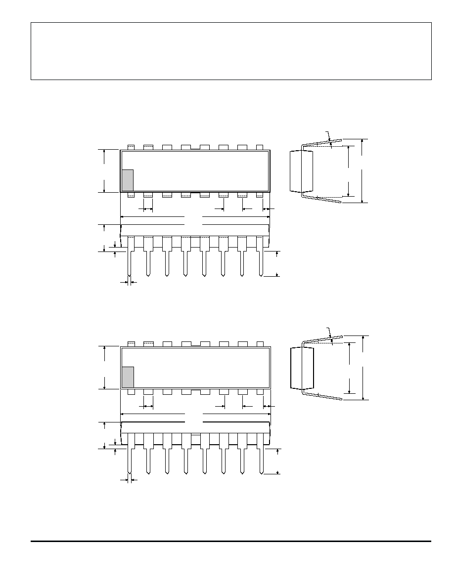
NOTES: 1. Exact body and lead configuration at vendor's option within limits shown.
2. Lead spacing tolerance is non-cumulative
3. Lead thickness is measured at seating plane or below.
4. Webbed lead frame. Leads 4, 5, 12, and 13 are internally one piece.
UDN2543B and UDQ2543B
Dimensions in Inches
(controlling dimensions)
Dimensions in Millimeters
(for reference only)
0.020
0.008
0.300
BSC
Dwg. MA-001-17A in
0.430
MAX
16
1
8
0.280
0.240
0.210
MAX
0.070
0.045
0.015
MIN
0.022
0.014
0.100
BSC
0.005
MIN
0.150
0.115
9
0.775
0.735
NOTE 4
0.508
0.204
7.62
BSC
Dwg. MA-001-17A mm
10.92
MAX
16
1
8
7.11
6.10
5.33
MAX
1.77
1.15
0.39
MIN
0.558
0.356
2.54
BSC
0.13
MIN
3.81
2.93
9
19.68
18.67
NOTE 4