 | –≠–ª–µ–∫—Ç—Ä–æ–Ω–Ω—ã–π –∫–æ–º–ø–æ–Ω–µ–Ω—Ç: UDN2961 | –°–∫–∞—á–∞—Ç—å:  PDF PDF  ZIP ZIP |

DISCONTINUED PRODUCT
-- FOR REFERENCE ONL
Y.
The UDN2961B and UDN2961W are 3.4 A half bridges designed
specifically for driving solenoid printheads, stepper motors, and dc
motors. The UDN2961B/W consists of a power source driver output,
a power sink driver output, a flyback recovery diode, internal current
sensing circuitry, and a user-selectable fixed off-time chopper circuit.
The output drivers are capable of sustaining 45 V with continuous
currents of
±
3.4 A and peak transient currents of
±
4 A permitted. The
outputs have been optimized for a low output saturation voltage
(typically 2.6 V total source plus sink drops at 3.4 A).
For output current control, load current is sensed internally and
limited by chopping the output driver(s) in a user-selectable fixed off-
time PWM mode. The maximum output current is determined by the
user's selection of a reference voltage. The MODE pin determines
whether the current control circuitry will chop in a slow current-decay
mode (only the source driver switching) or in a fast current-decay
mode (source and sink switching). A user-selectable blanking window
prevents false triggering of the current control circuitry during
chopping.
The UDN2961B is supplied in a 16-pin dual in-line plastic batwing
package with a copper lead-frame and heat sinkable tabs for improved
power dissipation capabilities. For higher power dissipation require-
ments, the UDN2961W is supplied in a 12-pin single in-line power tab
package.
FEATURES
s
3.4 A, 45 V Source and Sink Drivers
s
Internal Current Sensing
s
User-Selectable Fixed Off-Time PWM Current Control
s
Internal Flyback Diode
s
Low Output Saturation Voltage
s
Chip Enable
s
Fast or Slow Current-Decay Modes
s
Programmable Blanking Window
s
Internal Thermal Shutdown Circuitry
UDN2961B
HIGH-CURRENT HALF-BRIDGE
PRINTHEAD/MOTOR DRIVER--WITH INTERNAL
CURRENT SENSING AND CONTROL
ABSOLUTE MAXIMUM RATINGS
Supply Voltage, V
BB
. . . . . . . . . . . . . . 45 V
Output Current, I
OUT
(continuous) .
±
3.4 A
(t
w
20
µ
s, 10% duty cycle) . .
±
4.0 A
Logic Supply Voltage, V
CC
. . . . . . . . . 7.0 V
Input Voltage Range,
V
IN
. . . . . . . . . . . . . . . -0.3 V to +7.0 V
Package Power Dissipation,
P
D
. . . . . . . . . . . . . . . . . . . See Graph
Operating Temperature Range,
T
A
. . . . . . . . . . . . . . . . -20
∞
C to +85
∞
C
Junction Temperature, T
J
. . . . . . . +150
∞
C*
Storage Temperature Range,
T
S
. . . . . . . . . . . . . . . -55
∞
C to +150
∞
C
Output current rating may be restricted to a value
determined by system concerns and factors.
These include: system duty cycle and timing,
ambient temperature, and use of any heatsinking
and/or forced cooling. For reliable operation, the
specified maximum junction temperature should
not be exceeded.
* Fault conditions that produce excessive junction
temperature will activate device thermal shutdown
circuitry. These conditions can be tolerated, but
should be avoided.
Always order by complete part number:
Part Number Package
UDN2961B
16-Pin DIP
UDN2961W
12-Pin Power-Tab SIP
1
2
3
4
5
6
7
8
9
10
11
12
13
14
15
16
V
SOURCE OUT
EMITTER
SINK OUT
NC
GROUND
GROUND
CC
IN
ENABLE
RC
MODE
GROUND
GROUND
V
REF
V
BB
INPUT
CURRENT-
CONTROL
LOGIC
V
LOAD SUPPLY
LOGIC SUPPLY
BB
Dwg. PP-035
Data Sheet
29318.16*
2961
2961
HIGH-CURRENT
HALF-BRIDGE
PRINTHEAD/MOTOR DRIVER
115 Northeast Cutoff, Box 15036
Worcester, Massachusetts 01615-0036 (508) 853-5000
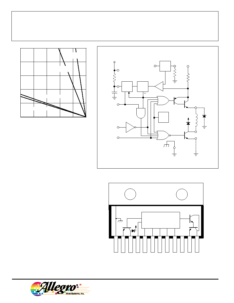
FUNCTIONAL BLOCK DIAGRAM
50
75
100
125
150
10
6
4
2
0
TEMPERATURE IN
∞
∞
∞
∞
C
8
25
Dwg. GP-032A
SUFFIX 'B', R = 43
∞
C/W
JA
SUFFIX 'W', R = 38
∞
C/W
JA
SUFFIX 'W',
R = 2.0
∞
C/W
JT
SUFFIX 'B',
R = 6.0
∞
C/W
JT
ALLOWABLE PACKAGE POWER DISSIPATION IN WATTS
UDN2961W
2940
TSD
R
S
LOW
TRIP
RC
SOURCE OUT
EMITTER
SINK OUT
ENABLE
INPUT
MODE
GROUND
R
C
Q
FLIP-
FLOP
REF
CIRCUIT
V
REF
CC
V
+5 V
BB
V
V
SENSE
BB
V
+
-
R
CV
ONE
SHOT
Dwg. FP-019A
1
2
3
4
5
6
7
8
9
10
11
12
EMITTER
INPUT
ENABLE
RC
MODE
SOURCE OUT
GROUND
SINK OUT
V
BB
V
CC
CURRENT-
CONTROL
LOGIC
LOGIC SUPPLY
LOAD SUPPLY
V
BB
V
REF
R
CV
Dwg. PP-036
Copyright © 1995, 1996 Allegro MicroSystems, Inc.

2961
HIGH-CURRENT
HALF-BRIDGE
PRINTHEAD/MOTOR DRIVER
www.allegromicro.com
Limits
Characteristic
Symbol
Test Conditions
Min.
Typ.
Max.
Units
Output Drivers
Output Leakage Current
I
CEX
V
EN
= 0.8 V, V
SOURCE
= 0 V
--
<-1.0
-100
µ
A
V
EN
= 0.8 V, V
SINK
= 45 V
--
<1.0
100
µ
A
Output Saturation Voltage
V
CE(SAT)
Source Driver, I
OUT
= -3.4 A
--
1.6
2.2
V
Source Driver, I
OUT
= -3.0 A
--
1.5
--
V
Sink Driver, I
OUT
= 3.4 A
--
1.0
1.4
V
Sink Driver, I
OUT
= 3.0 A
--
0.9
--
V
Output Sustaining Voltage
V
CE(sus)
I
OUT
=
±
3.4 A, L = 3 mH
45
--
--
V
Recovery Diode Leakage Current
I
R
V
R
= 45 V
--
<1.0
100
µ
A
Recovery Diode Forward Voltage
V
F
I
F
= 3.4 A
--
--
2.0
V
Motor Supply Current
I
BB(on)
V
EN
= 2.0 V, V
IN
= 0.8 V, No Load
--
--
70
mA
I
BB(off)
V
EN
= 0.8 V
--
--
2.5
mA
Output Rise Time
t
r
Source Driver, I
OUT
= -3.4 A
--
--
600
ns
Sink Driver, I
OUT
= 3.4 A
--
--
600
ns
Output Fall Time
t
f
Source Driver, I
OUT
= -3.4 A
--
--
600
ns
Sink Driver, I
OUT
= 3.4 A
--
--
600
ns
Control Logic
Logic Input Voltage
V
IN(1)
2.0
--
--
V
V
IN(0)
--
--
0.8
V
Logic Input Current
I
IN(1)
V
IN
= 5.0 V
--
--
10
µ
A
I
IN(0)
V
IN
= 0 V
--
--
-1.0
mA
Reference Input Current
I
REF
V
REF
= 5.0 V
--
--
50
µ
A
Transconductance
I
TRIP
/V
REF
V
REF
= 1.0 V
0.9
1.0
1.1
A/V
V
REF
= 3.2 V
0.9
1.0
1.1
A/V
Logic Supply Current
I
CC
V
EN
= 2.0 V, V
IN
= 0.8 V, No Load
--
--
160
mA
V
EN
= 0.8 V
--
--
15
mA
Turn On Delay
t
pd(on)
Source Driver
--
--
600
ns
Sink Driver
--
--
600
ns
Turn Off Delay
t
pd(off)
Source Driver
--
--
2.0
µ
s
Sink Driver
--
--
2.0
µ
s
Thermal Shutdown Temperature
T
J
--
165
--
∞
C
Negative current is defined as coming out of (sourcing) the specified device terminal.
ELECTRICAL CHARACTERISTICS at T
A
= +25
∞
C, V
BB
= 45 V,
V
CC
= 4.75 V to 5.25 V, R
CV
= 2940
(unless otherwise noted).

2961
HIGH-CURRENT
HALF-BRIDGE
PRINTHEAD/MOTOR DRIVER
115 Northeast Cutoff, Box 15036
Worcester, Massachusetts 01615-0036 (508) 853-5000
BB
V
V
SENSE
+
-
REF
CIRCUIT
BB
V
Dwg. EP-037
DRIVE CURRENT
RECIRCULATION (SLOW-DECAY MODE)
RECIRCULATION (FAST-DECAY MODE)
APPLICATIONS INFORMATION
The UDN2961B/W is a high current
half-bridge designed to drive a number of
inductive loads such as printer solenoids,
stepper motors, and dc motors. Load current
is sensed internally and is controlled by
pulse-width modulating (PWM) the output
driver(s) in a fixed off-time, variable-
frequency format. The peak current level is
set by the user's selection of a reference
voltage. A slow current-decay mode
(chopping only the source driver) or a fast
current-decay mode (chopping both the
source and sink drivers) can be selected via
the MODE pin.
PWM CURRENT CONTROL
A logic low on the MODE pin sets the
current-control circuitry into the slow-decay
mode. The RS flip-flop is set initially, and
both the source driver and the sink driver are
turned ON when the INPUT pin is at a logic
low. As current in the load increases, it is
sensed by the internal sense resistor until the
sense voltage equals the trip voltage of the
comparator. At this time, the flip-flop is reset
and the source driver is turned OFF. Over the
range of V
REF
= 0.8 V to 3.4 V, the output
current trip point transfer function is a direct
linear function of the reference voltage:
I
TRIP
= V
REF
To ensure an accurate chop current level
(
±
10%), an external 2940
±
1% resistor
(R
CV
) is used. The actual load current peak
will be slightly higher than the trip point
(especially for low-inductance loads) because
of the internal logic and switching delays
(typically 1.5
µ
s). After the source driver turns
OFF, the load current decays, circulating
through an external ground clamp diode, the
load, and the sink transistor. The source
driver's OFF time (and therefore the magni-
tude of the current decrease) is determined
by the one-shot's external RC timing compo-
nents:
t
OFF
= RC
within the range of 20 k
to 100 k
and 100 pF to 1000 pF. When the
one-shot times out, the flip-flop is set again, the source driver is re-
enabled, and the load current again is allowed to rise to the set peak
value and trip the comparator. This cycle repeats itself, maintaining the
average load current at the desired level.
ENABLE
INPUT
MODE
LOAD
CURRENT
RC
RC/2
I
TRIP
Dwg. WP-015

2961
HIGH-CURRENT
HALF-BRIDGE
PRINTHEAD/MOTOR DRIVER
www.allegromicro.com
A logic high on the MODE pin sets the
current-control circuitry into the fast-decay
mode. When the peak current threshold is
detected, the flip-flop is reset and both the
source driver and the sink driver turn OFF.
Load current decays quickly through the
external ground clamp diode, the load, and
the internal flyback diode. In the fast-
decay mode, the OFF time period is one-
half the time that is set by the external RC
network for the slow-decay mode:
t
OFF
=
The amount of ripple current, when
chopping in the fast-decay mode, is
considerably higher than when chopping in
the slow-decay mode.
The frequency of the PWM current
control is determined by the time required
for the load current to reach the set peak
threshold (a function of the load character-
istics and V
BB
) plus the OFF time of the
switching driver(s) (set by the external RC
components).
To prevent false resetting of the flip-
flop, due to switching transients and noise,
a blanking time for the comparator can be
set by the user where t
B
3600 x C in the
slow-decay mode or t
B
2400 x C in the
fast-decay mode. For C between 100 pF
and 1000 pF, t
B
is in
µ
s.
POWER CONSIDERATIONS
The UDN2961B/W outputs are opti-
mized for low power dissipation. The sink
driver has a maximum saturation voltage
drop of only 1.4 V at 3.4 A, while the
source driver has a 2.2 V drop at -3.4 A.
Device power dissipation is minimized in
the slow-decay mode, as the chopping
driver (the source driver) is ON for less
than 50% of the chop period. When the
source driver is OFF during a chop cycle,
power is dissipated on chip only by the sink
driver; the rest of the power is dissipated
through the external ground clamp diode.
In the fast-decay mode, the ON time of the
chopping drivers (both the source driver
and the sink driver) may be greater than 50%, and the power dissipa-
tion will be greater.
GENERAL
A logic low on the ENABLE pin prevents the source driver and the
sink driver from turning ON, regardless of the state of the INPUT pin or
the supply voltages. With the ENABLE pin high, a logic low on the
INPUT pin turns ON the output drivers.
To protect against inductive load voltage transients, an external
ground clamp diode is required. A fast-recovery diode is recom-
mended to reduce power dissipation in the UDN2961B/W. The blank-
ing time prevents false triggering of the current sense comparator,
which can be caused by the recovery current spike of the ground
clamp diode when the chopping source driver turns ON.
RC
2
1
2
3
4
5
6
7
8
9
10
11
12
13
14
15
16
V
CC
V
BB
CURRENT-
CONTROL
LOGIC
1
2
3
4
5
6
7
8
9
10
11
12
13
14
15
16
V
CC
CURRENT-
CONTROL
LOGIC
2940
±
1%
V
REF
INPUT
ENABLE
MODE
V
BB
V
BB
V
BB
R
C
R
C
Dwg. EP-038A
+5 V
+5 V
INPUT
47
µ
F
47
µ
F
2940
±
1%
BB
V
BB
V