Recommended for high-side switching applications that benefit from
separate logic and load grounds, these devices encompass load supply
voltages to 80 V and output currents to -500 mA. These 8-channel source
drivers are useful for interfacing between low-level logic and high-current
loads. Typical loads include relays, solenoids, lamps, stepper and/or servo
motors, print hammers, and LEDs.
All devices may be used with 5 V logic systems -- TTL, Schottky TTL,
DTL, and 5 V CMOS. The UDN2981A, UDN2982A, UDN2982LW, and
A2982SLW are electrically interchangeable, will withstand a maximum
output off voltage of 50 V, and operate to a minimum of 5 V; the UDN2983A,
UDN2984A, UDN2984LW, and A2984SLW drivers are electrically inter-
changeable, will withstand an output voltage of 80 V, and operate to a
minimum of 35 V. All devices in this series integrate input current limiting
resistors and output transient suppression diodes, and are activated by an
active high input.
The suffix `A' (all devices) indicates an 18-lead plastic dual in-line
package with copper lead frame for optimum power dissipation. Under
normal operating conditions, these devices will sustain 120 mA continuously
for each of the eight outputs at an ambient temperature of +50
∞C and a supply
of 15 V.
The suffix `LW' (UDN2982LW and UDN2984LW only) indicates an 18-
lead surface-mountable wide-body SOIC package; the A2982SLW and
A2984SLW are provided in a 20-lead wide-body SOIC package with im-
proved thermal characteristics.
The UDN2982A, UDN2982LW, A2982SLW, UDN2984A,
UDN2984LW, and A2984SLW drivers are also available for operation over
an extended temperature range to -40
∞C. To order, change the prefix `UDN'
to `UDQ' or the suffix `SLW' to `ELW'.
FEATURES
I TTL, DTL, PMOS, or CMOS Compatible Inputs
I 500 mA Output Source Current Capability
I Transient-Protected Outputs
I Output Breakdown Voltage to 80 V
I DIP or SOIC Packaging
8-CHANNEL SOURCE DRIVERS
Always order by complete part number, e.g.,
UDN2981A .
Note that all devices are not available in all package styles.
ABSOLUTE MAXIMUM RATINGS
at 25
∞C Free-Air Temperature
Output Voltage Range, V
CE
(UDN2981A, UDN2982A,
UDN2982LW, and A2982SLW) . . 5 V to 50 V
(UDN2983A, UDN2984A,
UDN2984LW, and A2984SLW) . 35 V to 80 V
Input Voltage, V
IN
(UDN2981A and UDN2983A) . . . . . . . . . 15 V
(UDN2982A, UDN2984A,
UDN2982LW, UDN2984LW,
A2982SLW, and A2984SLW) . . . . . . . . . 20 V
Output Current, I
OUT
. . . . . . . . . . . . . . -500 mA
Package Power Dissipation,
P
D
. . . . . . . . . . . . . . . . . . . . . . . See Graph
Operating Temperature Range,
T
A
. . . . . . . . . . . . . . . . . . . . -20
∞
C to +85
∞
C
Storage Temperature Range,
T
S
. . . . . . . . . . . . . . . . . . . -55
∞
C to +150
∞
C
Data Sheet
29310D*
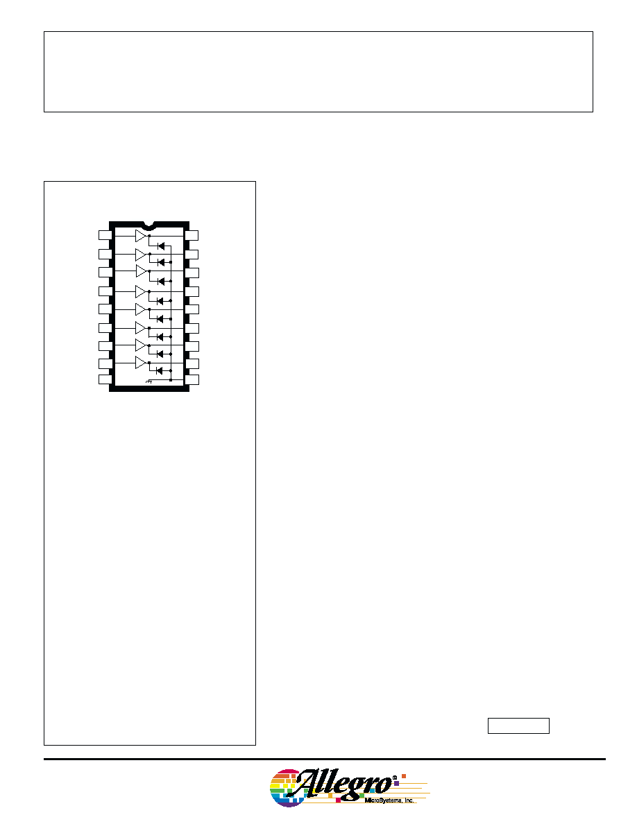
1
2
3
4
5
6
7
8
V
S
GND
11
12
13
14
15
16
17
18
UDN2981A thru UDN2984A
Dwg. No. A-10, 243
2981
THRU
2984
Note that the UDN2980A series (dual in-line
package) and UDN2980LW series (small-outline
IC package) are electrically identical and share a
common terminal number assignment.
2981
THRU
2984
8-CHANNEL
SOURCE DRIVERS
www.allegromicro.com
3
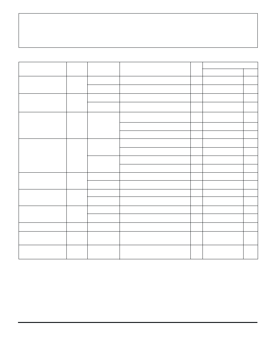
Applicable
Test
Limits
Characteristic
Symbol
Devices
Test Conditions
Fig.
Min.
Typ.
Max. Units
Output Leakage Current
I
CEX
2981/82
V
IN
= 0.4 V*, V
S
= 50 V, T
A
= +70
∞C
1
--
--
200
µA
2983/84
V
IN
= 0.4 V*, V
S
= 80 V, T
A
= +70
∞C
1
--
--
200
µA
Output Sustaining
V
CE(SUS)
2981/82
I
OUT
= -45 mA
--
35
--
--
V
Voltage
2983/84
I
OUT
= -70 mA
--
45
--
--
V
Collector-Emitter
V
IN
= 2.4 V, I
OUT
= -100 mA
2
--
1.6
1.8
V
Saturation Voltage
V
CE(SAT)
All
V
IN
= 2.4 V, I
OUT
= -225 mA
2
--
1.7
1.9
V
V
IN
= 2.4 V, I
OUT
= -350 mA
2
--
1.8
2.0
V
Input Current
2981/83A
V
IN
= 2.4 V
3
--
140
200
µA
I
IN(ON)
V
IN
= 3.85 V
3
--
310
450
µA
2982/84
V
IN
= 2.4 V
3
--
140
200
µA
V
IN
= 12 V
3
--
1.25
1.93
mA
Output Source Current
l
OUT
2981/83A
V
IN
= 2.4 V, V
CE
= 2.0 V
2
-350
--
--
mA
(Outputs Open)
2982/84
V
IN
= 2.4 V, V
CE
= 2.0 V
2
-350
--
--
mA
Supply Current
I
S
2981/82
V
IN
= 2.4 V*, V
S
= 50 V
4
--
--
10
mA
Leakage Current
2983/84
V
IN
= 2.4 V*, V
S
= 80 V
4
--
--
10
mA
Clamp Diode
I
R
2981/82
V
R
= 50 V, V
IN
= 0.4 V*
5
--
--
50
µA
Forward Voltage
2983/84
V
R
= 80 V, V
IN
= 0.4 V*
5
--
--
50
µA
Clamp Diode
V
F
All
I
F
= 350 mA
6
--
1.5
2.0
V
Turn-On Delay
t
ON
All
0.5 E
IN
to 0.5 E
OUT
, R
L
= 100
,
--
--
1.0
2.0
µs
V
S
= 35 V
Turn-Off Delay
t
OFF
All
0.5 E
IN
to 0.5 E
OUT
, R
L
= 100
,
--
--
5.0
10
µs
V
S
= 35 V, See Note
ELECTRICAL CHARACTERISTICS at T
A
= +25
∞
C (unless otherwise specified).
NOTES: Turn-off delay is influenced by load conditions. Systems applications well below the specified output loading may require
timing considerations for some designs, i.e., multiplexed displays or when used in combination with sink drivers in a totem
pole configuration.
Negative current is defined as coming out of (sourcing) the specified device terminal.
* All inputs simultaneously.
Complete part number includes a prefix (A or UDN) and a suffix (A or SLW) as follows:
UDN2981A,
UDN2982A, UDN2982LW, or A2982SLW,
UDN2983A,
UDN2984A, UDN2984LW, or A2984SLW.

2981
THRU
2984
8-CHANNEL
SOURCE DRIVERS
www.allegromicro.com
5
Allowable peak collector current
as a function of duty cycle
Series UDN2980A
100
V = 35 V
8
7
6
4
5
NUMBER OF OUTPUTS
CONDUCTING
SIMULTANEOUSLY
90
80
70
60
50
40
30
20
10
0
0
50
100
150
200
250
300
350
400
450
500
RECOMMENDED MAXIMUM OUTPUT CURRENT
ALLOW
ABLE PEAK COLLECT
OR CURRENT
IN mA
A
T
50
∞
C
PER CENT DUTY CYCLE
S
3
100
V = 35 V
8
7
6
4
5
NUMBER OF OUTPUTS
CONDUCTING
SIMULTANEOUSLY
90
80
70
60
50
40
30
20
10
0
0
50
100
150
200
250
300
350
400
450
500
RECOMMENDED MAXIMUM OUTPUT CURRENT
ALLOW
ABLE PEAK COLLECT
OR CURRENT
IN mA
A
T
70
∞
C
PER CENT DUTY CYCLE
S
3
Dwg. No. A-11,111B
Dwg. No. A-11,106B
UDN2981A and UDN2982A
100
V = 15 V
8
7
6
4
5
NUMBER OF OUTPUTS
CONDUCTING
SIMULTANEOUSLY
90
80
70
60
50
40
30
20
10
0
0
50
100
150
200
250
300
350
400
450
500
RECOMMENDED MAXIMUM OUTPUT CURRENT
ALLOW
ABLE PEAK COLLECT
OR CURRENT
IN mA
A
T
50
∞
C
PER CENT DUTY CYCLE
S
3
100
V = 15 V
8
7
6
4
5
NUMBER OF OUTPUTS
CONDUCTING
SIMULTANEOUSLY
90
80
70
60
50
40
30
20
10
0
0
50
100
150
200
250
300
350
400
450
500
RECOMMENDED MAXIMUM OUTPUT CURRENT
ALLOW
ABLE PEAK COLLECT
OR CURRENT
IN mA
A
T
70
∞
C
PER CENT DUTY CYCLE
S
3
Dwg. No. A-11,107B
Dwg. No. A-11,108B

