 | –≠–ª–µ–∫—Ç—Ä–æ–Ω–Ω—ã–π –∫–æ–º–ø–æ–Ω–µ–Ω—Ç: UDN2987 | –°–∫–∞—á–∞—Ç—å:  PDF PDF  ZIP ZIP |
2987
8-CHANNEL
SOURCE DRIVER
8-CHANNEL SOURCE DRIVER
WITH OVER-CURRENT PROTECTION
Providing over-current protection for each of its eight sourcing
outputs, the UDN2987A and UDN2987LW drivers are used as an
interface between standard low-level logic and relays, motors, sole-
noids, LEDs, and incandescent lamps. The device includes thermal
shutdown and output transient protection/clamp diodes for use with
sustaining voltages to 35 V.
In these drivers, each channel includes a latch to turn OFF that
channel if the maximum channel current is exceeded. All channels are
disabled if the thermal shutdown is activated. A common FAULT
output is used to indicate either chip thermal shutdown or any over-
current condition. All outputs are enabled by pulling the common OE/
R input high. When OE/R is low, all outputs are inhibited and the eight
latches are reset.
Under normal operating conditions, each of eight outputs will
source in excess of 100 mA continuously at an ambient temperature of
25
∞
C and a supply of 35 V. The over-current fault circuit will protect
the device from short-circuits to ground with supply voltages of up to
35 V.
The inputs are compatible with 5 V and 12 V logic systems--TTL,
Schottky TTL, DTL, PMOS, and CMOS. In all cases, the output is
switched ON by an active high input level. The UDN2987A is supplied
in a 20-pin dual in-line plastic package; the UDN2987LW is supplied in
a 20-lead small-outline plastic package.
FEATURES
s
350 mA Output Source Current
s
Over-Current Protected
s
Internal Ground Clamp Diodes
s
Output Breakdown Voltage 35 V, Minimum
s
TTL, DTL, PMOS, or CMOS Compatible Inputs
s
Internal Thermal Shutdown
s
Automotive Capable
Data Sheet
29310.4A
Always order by complete part number:
Part Number
Package
UDN2987A
20-Pin DIP
UDN2987LW
20-Lead Wide-Body SOIC
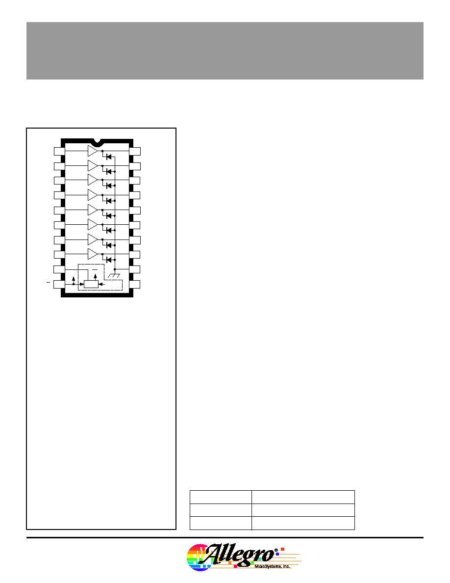
Note that the UDN2987A (DIP) and the UDN2987LW
(SOIC) are electrically identical and share a common
terminal number assignment.
Dwg. PP-067
V
S
1
2
3
4
5
6
7
8
14
15
16
17
18
19
20
9
10
11
12
13
GROUND
OUT
IN
FAULT
OE/R
1
OE
N
OE
SENSE
N
FF
x8
OUT 2
OUT 3
OUT 4
OUT 5
OUT 6
OUT 7
OUT 8
1
IN 2
IN 3
IN 4
IN 5
IN 6
IN 7
IN 8
2987
ABSOLUTE MAXIMUM RATINGS
at T
A
= +25
∞
C
Driver Supply Voltage, V
S
..................... 35 V
Output Sustaining Voltage, V
CE(sus)
...... 35 V
Continuous Output Current,
I
OUT
........................................ -500 mA*
FAULT Output Voltage, V
CE
................. 35 V
FAULT Output Current, l
C
................. 30 mA
Input Voltage, V
IN
................................. 15 V
Package Power Dissipation,
P
D
........................................ See Graph
Operating Temperature Range,
T
A
................................. -20
∞
C to +85
∞
C
Storage Temperature Range,
T
S
............................... -55
∞
C to +150
∞
C
* Outputs are disabled at approximately -500 mA
per driver.
2987
8-CHANNEL
SOURCE DRIVER
115 Northeast Cutoff, Box 15036
Worcester, Massachusetts 01615-0036 (508) 853-5000
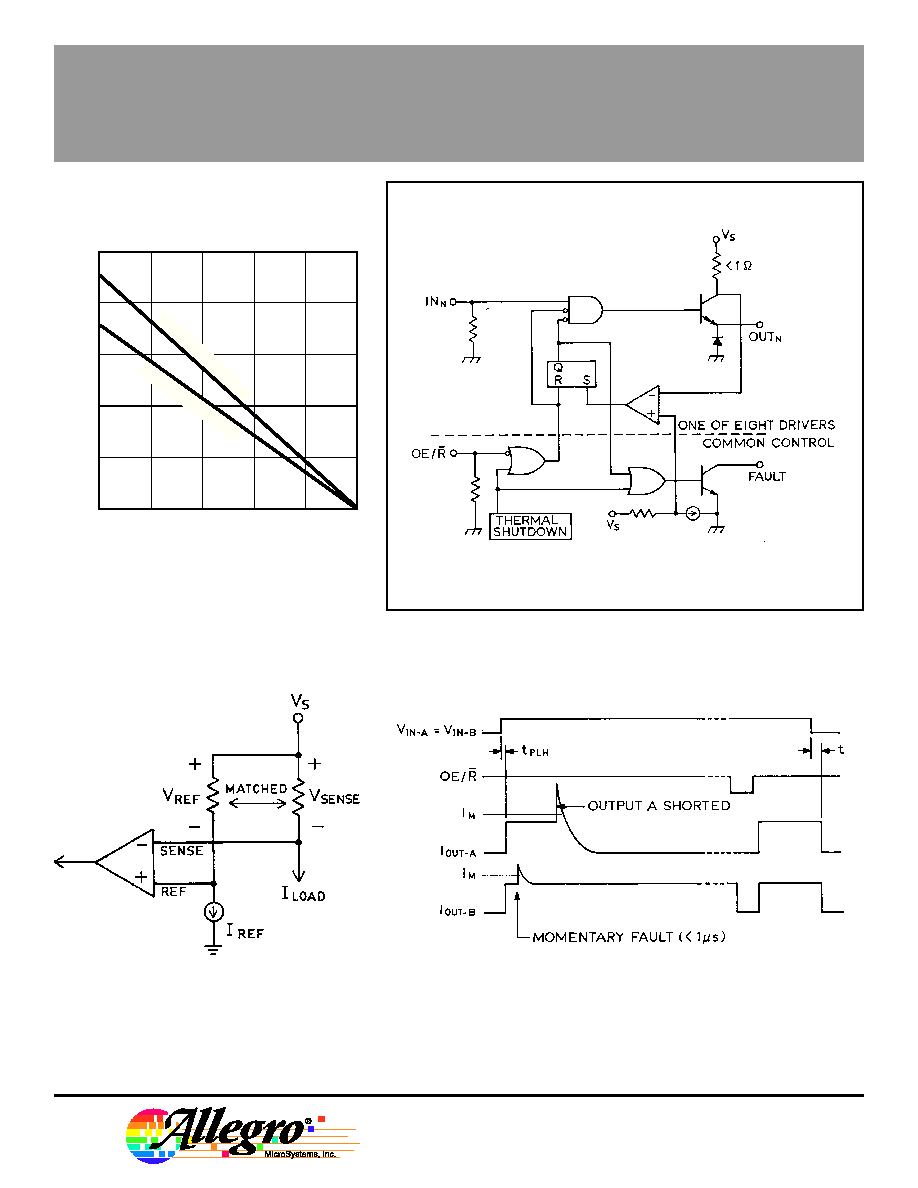
FUNCTIONAL BLOCK DIAGRAM
OUTPUT CURRENT WAVESHAPES
OVER-CURRENT FAULT SENSE
Dwg. No. A-13,293
Dwg. No. A-13,292
Dwg. No. A-13,286
PHL
50
75
100
125
150
2.5
0.5
0
ALLOWABLE PACKAGE POWER DISSIPATION IN WATTS
AMBIENT TEMPERATURE IN
∞
C
2.0
1.5
1.0
25
Dwg. GS-004A
SUFFIX 'LW', R = 70
∞
C/W
JA
SUFFIX 'A', R = 55
∞
C/W
JA
Copyright © 1987, 1997, Allegro MicroSystems, Inc.
2987
8-CHANNEL
SOURCE DRIVER
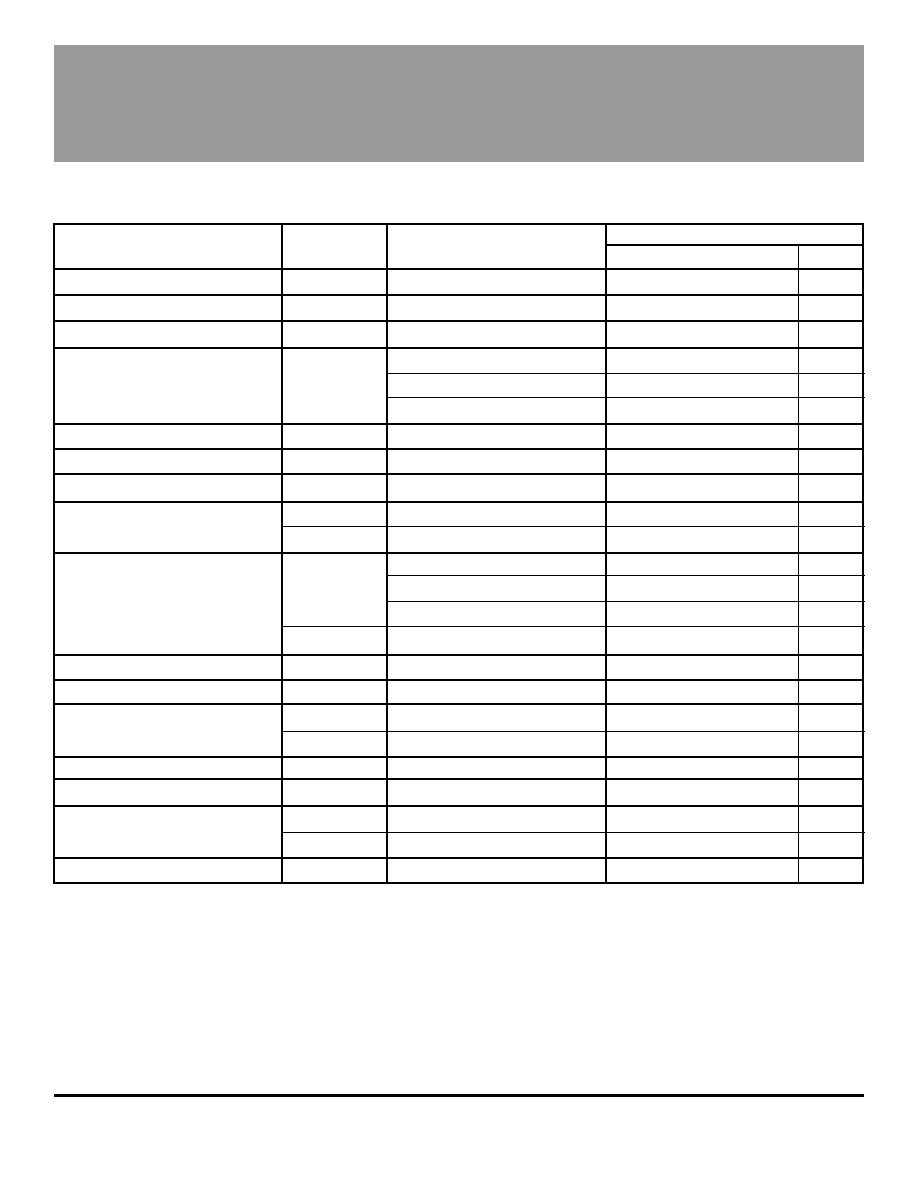
ELECTRICAL CHARACTERISTICS at T
A
= 25
∞
C, V
OE
= 2.4 V, V
S
= 35 V
(unless otherwise noted).
Limits
Characteristic
Symbol
Test Conditions
Min.
Typ.
Max.
Units
Functional Supply Range
V
S
7.0
--
35
V
Output Leakage Current
I
CEX
V
IN
= 0.4 V*
--
<-5.0
-200
µ
A
Output Sustaining Voltage
V
OUT(sus)
I
OUT
= -350 mA, L = 2.0 mH
35
--
--
V
Output Saturation Voltage
V
OUT(SAT)
V
IN
= 2.4 V, I
OUT
= -100 mA
--
1.6
1.8
V
V
IN
= 2.4 V, I
OUT
= -225 mA
--
1.7
1.9
V
V
IN
= 2.4 V, I
OUT
= -350 mA
--
1.8
2.0
V
Channel Shutdown Threshold
I
M
V
IN
= 2.4 V
-370
-500
--
mA
FAULT Leakage Current
I
CEX
V
CC
= 35 V
--
<1.0
100
µ
A
FAULT Saturation Voltage
V
CE(SAT)
I
C
= 30 mA
--
0.3
0.8
V
Input Voltage
V
IN(ON)
2.4
--
--
V
V
IN(OFF)
--
--
0.4
V
Input Current
I
IN(ON)
V
IN
= 2.4 V
--
125
170
µ
A
V
IN
= 5.0 V
--
840
1020
µ
A
V
IN
= 12 V
--
1500
1800
µ
A
I
IN(OFF)
V
IN
= 0.4 V
--
--
15
µ
A
Clamp Diode Leakage Current
I
R
V
R
= 35 V, T
A
= 70
∞
C
--
--
50
µ
A
Clamp Diode Forward Voltage
V
F
I
F
= 350 mA
--
1.5
1.8
V
Supply Current
I
S(ON)
V
IN
= 2.4 V*, Outputs Open
--
13
18
mA
I
S(OFF)
V
IN
= 0.4 V*
--
8.0
12
mA
Thermal Shutdown
T
J
--
165
--
∞
C
Thermal Hysteresis
T
J
--
15
--
∞
C
Propagation Delay Time
t
PLH
R
L
= 100
--
0.3
0.6
µ
s
t
PHL
R
L
= 100
--
2.0
4.0
µ
s
Dead Time
t
d
--
1.0
--
µ
s
*AII inputs simultaneously.
2987
8-CHANNEL
SOURCE DRIVER
115 Northeast Cutoff, Box 15036
Worcester, Massachusetts 01615-0036 (508) 853-5000
APPLICATIONS INFORMATION
AND CIRCUIT DESCRIPTION
As with all power integrated circuits, the UDN2987A
and UDN2987LW have a maximum allowable output
current rating. The 500 mA rating does not imply that
operation at that value is permitted or even obtainable.
The channel output current trip point is specified as -370
mA, minimum; therefore, attempted operation at current
levels greater than -370 mA may cause a fault indication
and channel shutdown. The device is tested at a maxi-
mum of -350 mA and that is the recommended maximum
output current per driver. It provides protection for current
overloads or shorted loads up to 35 V.
All outputs are enabled by pulling the OE/R input high.
When OE/R is low or allowed to float (internal pull-down),
all outputs are inhibited and the latches are reset. Note
that the RESET pulse duration (OE/R low) should be
at least 1
µ
s. This will ensure safe operation under
attempted RESET conditions with a shorted load. The
latches are also reset during power up, regardless of the
state of the OE/R input.
The load current causes a small voltage drop across
the internal low-value sense resistor. This voltage is
compared to the voltage drop across a reference resistor
with a constant current. The two resistors are matched to
eliminate errors due to manufacturing tolerances or
temperature effects. Each channel includes a comparator
and its own latch. An over-current fault (V
SENSE
> V
REF
)
will set the affected latch and shut down only that channel.
All other channels will continue to operate normally. The
latch includes a 1
µ
s delay (t
d
) to prevent unwanted
triggering due to crossover currents generated when
switching inductive loads. For an abrupt short circuit, the
delay and output switching times will allow a brief,
permissable current in excess of the trip current before the
output driver is turned OFF.
A common thermal shutdown disables all outputs
if the chip temperature exceeds +165
∞
C. At thermal
shutdown, all latches are reset. The outputs are disabled
until the chip cools down to about +150
∞
C (thermal
hysteresis).
A common open-collector FAULT output is used to
indicate any channel over-current condition or chip
thermal shutdown.
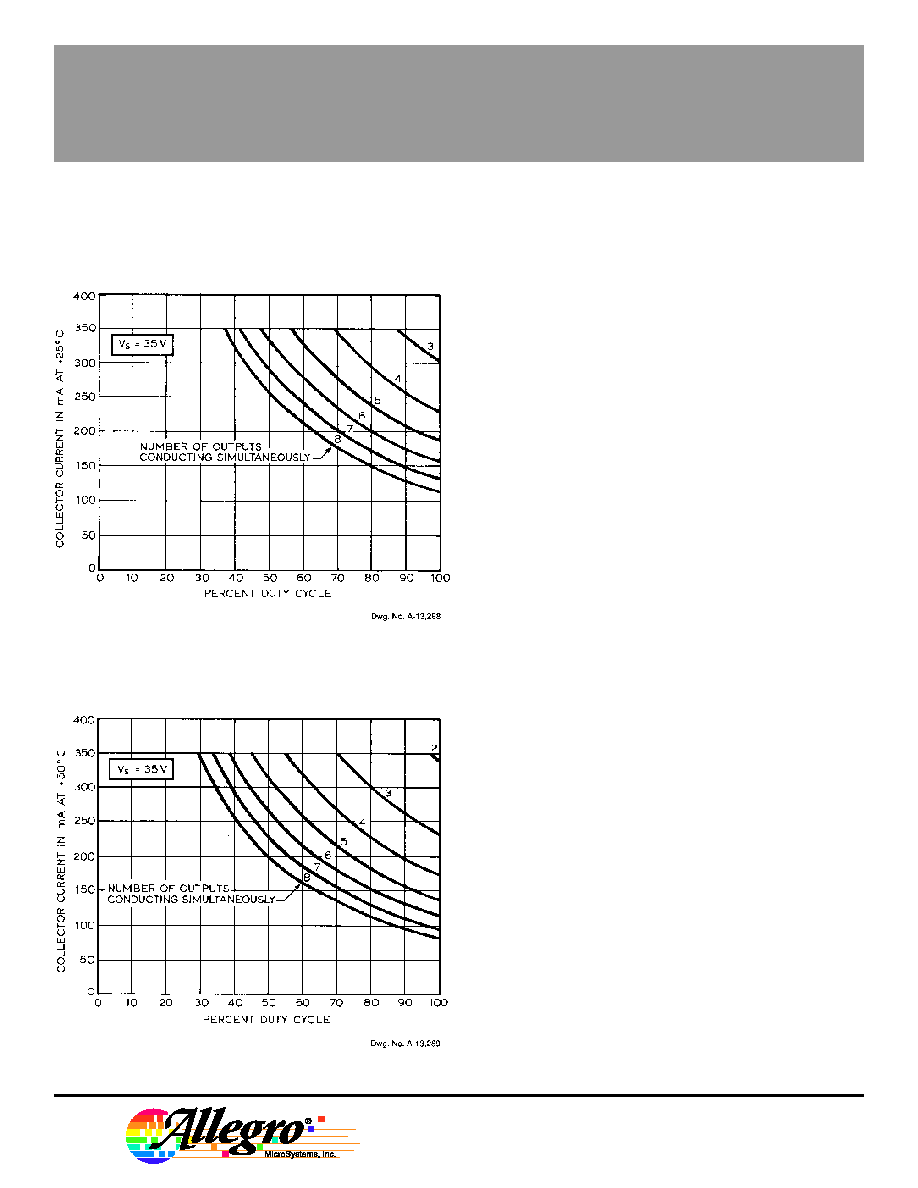
ALLOWABLE OUTPUT CURRENT
AS A FUNCTION OF DUTY CYCLE
(UDN2987A shown, multiply by 78% for UDN2987LW)
At +25
∞
C
At +50
∞
C
2987
8-CHANNEL
SOURCE DRIVER
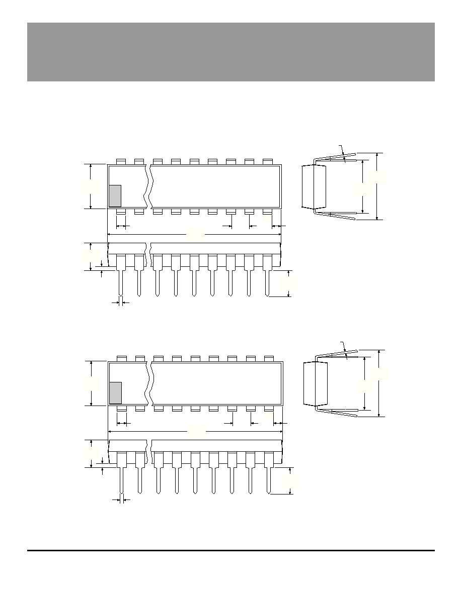
NOTES: 1. Exact body and lead configuration at vendor's option within limits shown.
2. Lead spacing tolerance is non-cumulative.
3. Lead thickness is measured at seating plane or below.
Dimensions in Millimeters
(for reference only)
UDN2987A
Dimensions in Inches
(controlling dimensions)
0.014
0.008
0.300
BSC
Dwg. MA-001-20 in
0.430
MAX
20
1
10
0.280
0.240
0.210
MAX
0.070
0.045
0.015
MIN
0.022
0.014
0.100
BSC
0.005
MIN
0.150
0.115
11
1.060
0.980
0.355
0.204
7.62
BSC
Dwg. MA-001-20 mm
10.92
MAX
20
1
10
7.11
6.10
5.33
MAX
1.77
1.15
0.39
MIN
0.558
0.356
2.54
BSC
0.13
MIN
3.81
2.93
11
26.92
24.89