Requiring a minimum of external components, the UDN3625M
and UDN3626M are monolithic ICs that provide single-chip control
and direct drive solutions for many small, single-phase, unipolar
brushless dc motor applications. Integrated into the ICs are a high-
sensitivity Hall-effect sensor, control and commutating logic, a stable
voltage regulator, extensive self and system protective functions, and
two high-current saturated npn outputs. Both ICs include thermal
shutdown, output over-current limiting, and output transient protection/
flyback diodes. The UDN3625M is nominally for 12 V motor applica-
tions while the UDN3626M is better suited to 24 V motors.
Output over-current limiting (relating to startup surge or a locked
rotor condition) and short-circuit protection are provided by an internal
current-sense resistor. The maximum (default) output load current is
typically 1.3 A for the UDN3625M or 600 mA for the UDN3626M,
but may be decreased by user selection of an external low-wattage
resistor.
A separate low-level output provides tachometer capability for
motor speed control or sensing a locked rotor condition. With appro-
priate external logic, pulse-width modulated (PWM) speed control can
be accomplished at the output current adjust pin.
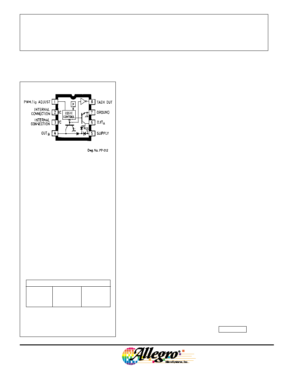
These sensor/drivers are supplied in an 8-pin mini-DlP plastic
package with a copper leadframe for increased package power
handling capability.
P
OWER
H
ALL
�
SENSOR/DRIVERS
FOR BRUSHLESS DC MOTORS
Always order by complete part number, e.g., UDN3625M .
See Maximum Ratings at left.
Supply Voltage, V
CC
. . . . . . . . . . See Table
Output Current, I
O
. . . . . . . . . . . . See Table
PWM Current Control Voltage,
V
ADJ
. . . . . . . . . . . . . See Applications
Magnetic Flux Density, B . . . . . . Unlimited
Package Power Dissipation,
P
D
. . . . . . . . . . . . . . . . . . . . See Graph
Operating Temperature Range,
T
A
. . . . . . . . . . . . . . . . . -20
�
C to +85
�
C
Storage Temperature Range,
T
S
. . . . . . . . . . . . . . . . -65
�
C to +150
�
C
Output current rating will be limited by
ambient temperature, supply voltage, and
duty cycle. Under any set of conditions, do
not exceed a junction temperature of
+150
�
C.
UDN3625M
UDN3626M
V
CC(MAX)
14 V
26 V
I
O(CONT)
1.0 A
0.45 A
I
O(PEAK)
1.6 A
0.75 A
ABSOLUTE MAXIMUM RATINGS
Data Sheet
27690A
FEATURES
s
900 mA /12 V or 400 mA /24 V Operation
s
Speed-Control (PWM) Capability
s
Locked-Rotor Indication
s
Minimum External Components
s
Over-Current Protected
s
Thermal Protection
s
Enhanced Reliability
s
Reduced Cost
3625
AND
3626
CONTACT FACTORY
for availability
and latest information
3625
AND
3626
P
OWER
H
ALL
�
SENSOR/DRIVERS FOR
BRUSHLESS DC MOTORS
115 Northeast Cutoff, Box 15036
Worcester, Massachusetts 01615-0036 (508) 853-5000
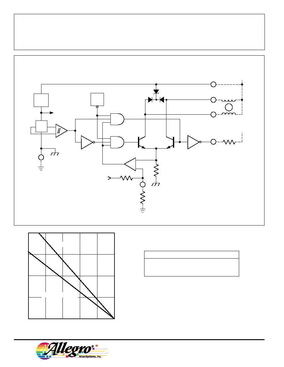
TACH
OUT
SUPPLY
OUT
B
Dwg. FP-005-1
8
6
4
5
7
1
REG.
TSD
GROUND
X
R
ADJ
V
+V
S
OUT
A
PWM/I
ADJUST
O
FUNCTIONAL BLOCK DIAGRAM
TRUTH TABLE
Mag. FieldPWM/I
O
ADJ
OUT
A
OUT
B
> +B
OP
Open
Low
High
> -B
OP
Open
High
Low
Any
<0.3 V
High
High
50
75
100
125
150
0.5
0
ALLOWABLE PACKAGE POWER DISSIPATION IN WATTS
TEMPERATURE IN
�
C
2.0
1.5
1.0
25
Dwg. GP-009-1B
R = 55
�
C/W
JC
FREE AIR, R = 80
�
C/W
JA
Copyright � 1988, 1995, Allegro MicroSystems, Inc.

3625
AND
3626
P
OWER
H
ALL
�
SENSOR/DRIVERS FOR
BRUSHLESS DC MOTORS
ELECTRICAL CHARACTERISTICS at T
A
= +25
�
C, R
ADJ
=
, Over Operating Voltage Range
(unless otherwise noted).
Output Clamp Voltage
(Test Fig. 1)
Output Clamp Voltage
Supply Current
(Test Fig. 1)
(Test Fig. 2)
(Test Fig. 2)
Limits
Characteristic
Symbol
Test Conditions
Min.
Typ.
Max.
Units
UDN3625M
Operating Voltage Range
V
S
6.5
12
14
V
Output Leakage Current
I
O
V
CC
= V
O
= 24 V
--
--
100
�
A
Output Breakdown Voltage
V
(BR)CEX
V
CC
= 24 V, l
O
= 10 mA*
34
--
--
V
Output Saturation Voltage
V
O(SAT)
I
O
= 450 mA, V
S
= 6.5 V
--
0.25
0.4
V
I
O
= 900 mA, V
S
= 12 V
--
0.5
0.8
V
Output Current Limit
I
O
MAX
R
ADJ
=
, V
O
= 2 V
1.0
1.3
1.6
A
V
CL
I
CL
= 10 mA, V
CC
= 0
11
12
13
V
I
CL
= 450 mA=, V
CC
= 0
13
14
15
V
Output Switching Time
t
PLH
50% V
ADJ
to V
O
= 3.0 V, l
O
= 450 mA
--
--
5.0
�
s
l
CC
R
ADJ
=
, V
S
= 14 V, One Output ON
--
30
38
mA
R
ADJ
= 0
, V
S
= 14 V, Outputs OFF
--
8.0
10
mA
UDN3626M
Operating Voltage Range
V
S
24
26
V
Output Leakage Current
l
O
V
CC
= V
O
= 30 V
--
--
100
�
A
Output Breakdown Voltage
V
(BR)CEX
V
CC
= 30 V, l
O
= 10 mA*
50
--
--
V
Output Saturation Voltage
V
O(SAT)
l
O
= 250 mA, V
S
= 6.5 V
--
0.15
0.3
V
l
O
= 400 mA, V
S
= 24 V
--
0.3
0.5
V
Output Current Limit
l
O
MAX
R
ADJ
=
, V
O
= 2 V
450
600
750
mA
V
CL
I
CL
= 10 mA, V
CC
= 0
17
18
20
V
I
CL
= 250 mA, V
CC
= 0
19
20
22
V
Output Switching Time
t
PLH
50% V
ADJ
to V
O
= 3.0 V, l
O
= 250 mA
--
--
5.0
�
s
Supply Current
l
CC
R
ADJ
=
, V
S
= 26 V, One Output ON
--
--
24
mA
R
ADJ
= 0
, V
S
= 26 V, Outputs OFF
--
8.0
10
mA
Continued next page...
* l
O
is almost entirely Zener clamp current.
Pulse test.
Dependent on value of external series Zener diode (see Applications), 6.5 V without a Zener diode.
3625
AND
3626
P
OWER
H
ALL
�
SENSOR/DRIVERS FOR
BRUSHLESS DC MOTORS
115 Northeast Cutoff, Box 15036
Worcester, Massachusetts 01615-0036 (508) 853-5000
ELECTRICAL CHARACTERISTICS continued
Limits
Characteristic
Symbol
Test Conditions
Min.
Typ.
Max.
Units
Both
Operate Point�
B
OP
--
�
100
�
150
G
Hysteresis
B
H
--
200
--
G
Output Current Limit Ratio
l
O
/l
O
MAX
R
ADJ
= 39 k
--
0.75
--
--
R
ADJ
= 17 k
--
0.50
--
--
R
ADJ
= 10 k
--
0.25
--
--
PWM Control Current
I
ADJ
V
ADJ
= 0
--
-350
-500
�
A
Tach Output Leak. Current
I
T
V
T
= 14 V
--
--
10
�
A
Tach Output Sat. Voltage
V
T(SAT)
I
T
= 750
�
A
--
0.2
0.4
V
Thermal Shutdown
T
J
��
165
--
�
C
Thermal Hysteresis
T
J
��
10
--
�
C
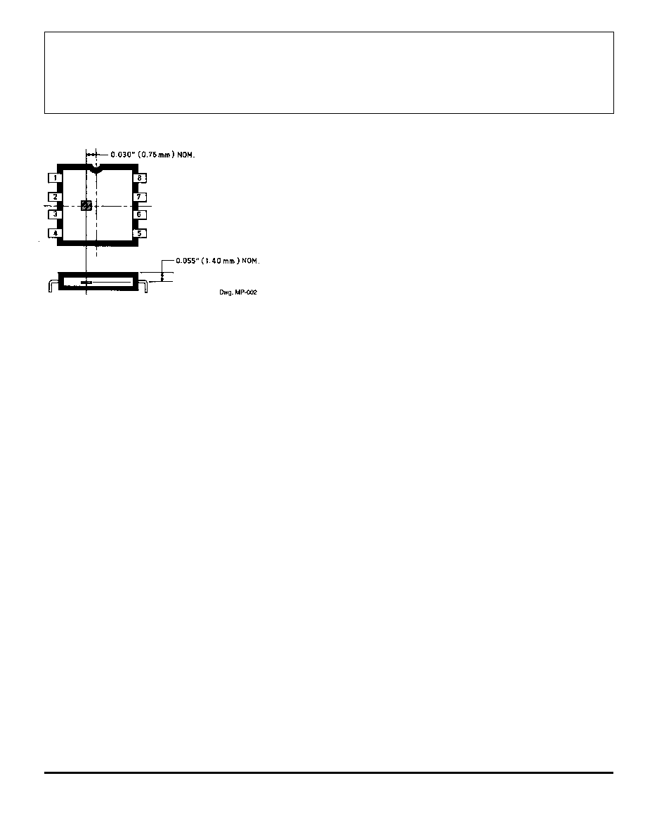
� Magnetic flux density is measured at most sensitive area of device, nominally located 0.055" (1.40 mm) below the top of the package.
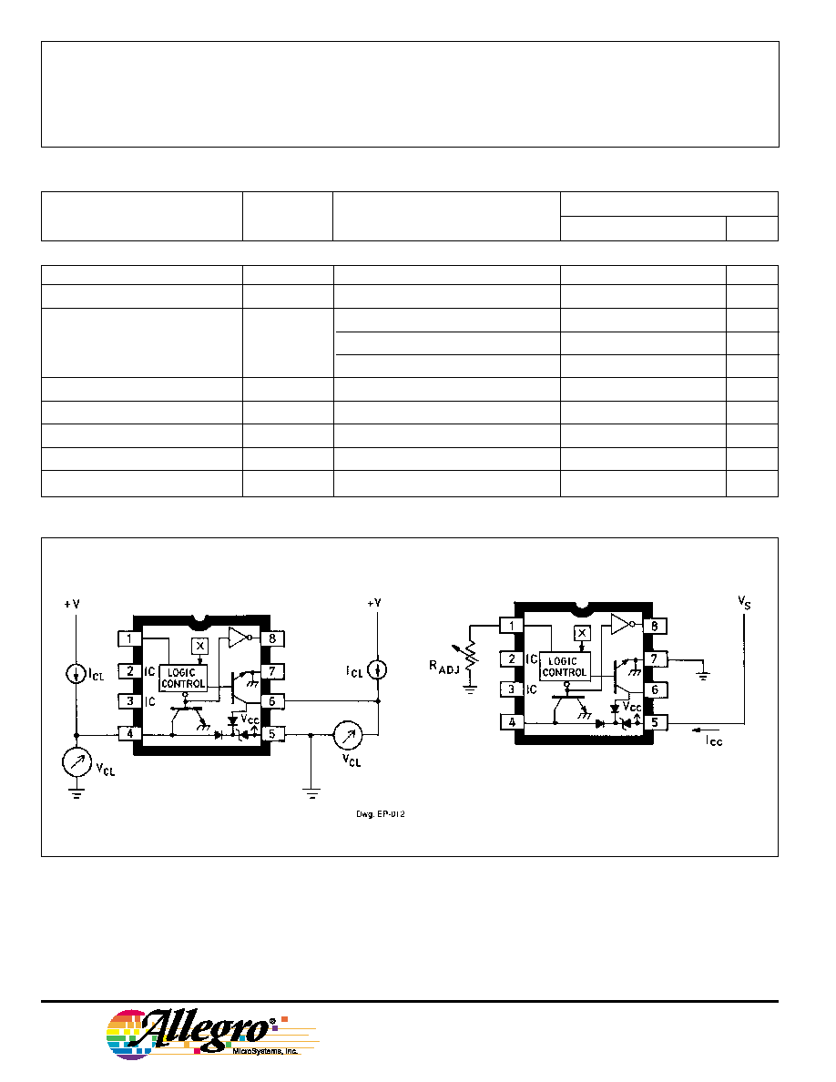
OUTPUT CLAMP VOLTAGE TEST
(ONE OUTPUT TESTED AT A TIME)
SUPPLY CURRENT TEST
Dwg. No. EP-013
TEST FIG. 2
TEST FIG. 1
3625
AND
3626
P
OWER
H
ALL
�
SENSOR/DRIVERS FOR
BRUSHLESS DC MOTORS
SENSOR LOCATION
APPLICATIONS INFORMATION
Power Dissipation. Care should be taken in evaluating the package power
dissipation of these devices. Total power dissipated by the device will consist
of power due to the internal regulator, logic and drive circuitry (I
CC
x V
CC
),
power due to the output drivers (I
O
x V
O(SAT)
), and power due to the clamp
circuitry (I
CL
x V
CL
x duty cycle).
For example:
I
CC
x V
CC
= 38 mA (max) x 14 V = 532 mW (max)
I
O
x V
O(SAT)
= 450 mA x 0.4 V (max) = 180 mW (max)
I
CL
x V
CL
x duty cycle = 450 mA x 15 V (max) x 1% = 67.5 mW (max)
Total package power dissipation = 779.5 mW (max)
Some of the power dissipated by the device (I
CC
x V
CC
) can be reduced
by inserting a Zener diode in the supply line (Z
A
in the figure). Note that the
voltage at the V
CC
pin under worst-case conditions must be greater than the
minimum operating voltage (6.5 V).
Transient Protection. A note of caution concerns negative (below ground)
excursions of the outputs. In application, the coupling of the two motor
windings can provide for just such a case. Reducing the coupling between
windings will help, but ground clamp diodes or diodes in series with the
motor windings might be required (D
C
or D
S
in the figure). Most small
brushless motors will not require these diodes.
System requirements usually utilize a diode type of reverse-polarity
protection. If series diode protection is used with an inductive load (the usual
fan application), a Zener clamp between V
S
and ground (Z
B
in the figure) is
required. The Zener voltage must be greater than the supply voltage but less
than the rated maximum allowable supply voltage.
With diode reverse-polarity protection, a high-impedance supply, or a
switched supply line, high-voltage spikes will be generated (especially with
high-current or high-inductance loads) during normal operation, coasting, or
immediately after turn-off. In these situations, a Zener clamp (Z
B
) from V
S
to
ground will be required.
Over-Current Adjust Pin. The over-current limit may be reduced from the
default value (I
O
MAX) by selection of an external resistor (R
ADJ
) at the
PWM/I
O
ADJ pin.