PROTECTED
QUAD POWER DRIVER
Providing improved output current limiting, the UDK/UDN/
UDQ2549B and UDK/UDN/UDQ2549EB quad power drivers combine
AND logic gates and high-current bipolar outputs with complete output
protection. Each of the four outputs will sink 600 mA in the on state.
The outputs have a minimum breakdown voltage (load dump) of 60 V
and a sustaining voltage of 40 V. The inputs are compatible with TTL
and 5 V CMOS logic systems.
Over-current protection for each channel has been designed into
these devices and is activated at approximately 1 A. It protects each
output from short circuits with supply voltages up to 25 V. When an
output current trip point is reached, that output stage is driven linearly
resulting in a reduced output current level. If an over-current or short
circuit condition continues, the thermal limiting circuits will first sense
the rise in junction temperature and then the rise in chip temperature,
further decreasing the output current. Under worst-case conditions,
the six devices in this family will tolerate short-circuits on all outputs,
simultaneously.
These devices can be used to drive various loads including
incandescent lamps (without warming or limiting resistors) or inductive
loads such as relays, solenoids, or dc stepping motors.
The suffix `B' devices are 16-pin power DIPs while the suffix `EB'
devices are 28-lead power PLCCs for surface-mount applications.
Both packages are of batwing construction to provide for maximum
package power dissipation.
FEATURES
I 600 mA Output Current per Channel
I Independent Over-Current Protection for Each Driver
I Thermal Protection for Device and Each Driver
I Low Output-Saturation Voltage
I Integral Output Flyback Diodes
I TTL and 5 V CMOS Compatible Inputs
I Pin-Compatible With UDN2543B/EB
ABSOLUTE MAXIMUM RATINGS
at T
A
= 25
�
C
Output Voltage, V
OUT
. . . . . . . . . . . . . 60 V
Over-Current Protected Output Voltage,
V
OUT
. . . . . . . . . . . . . . . . . . . . . . . 25 V
Output Current, I
OUT
. . . . . . . . . . . . . 1.0 A*
Supply Voltage, V
CC
. . . . . . . . . . . . . . 7.0 V
Input Voltage, V
IN
or V
EN
. . . . . . . . . . 7.0 V
Package Power Dissipation,
P
D
. . . . . . . . . . . . . . . . . . . . See Graph
Operating Temperature Range, T
A
Prefix `UDK' . . . . . . . -40
�
C to +125
�
C
Prefix `UDN' . . . . . . . . -20
�
C to +85
�
C
Prefix `UDQ' . . . . . . . . -40
�
C to +85
�
C
Storage Temperature Range,
T
S
. . . . . . . . . . . . . . . -55
�
C to +150
�
C
*Outputs are peak current limited at approximately
1.0 A per driver. See Circuit Description and
Applications for further information.
Always order by complete part number: a prefix to indicate operating
temperature range + the basic four-digit part number + a suffix to
indicate package style, e.g., UDK2549EB .
UDx2549B
Data Sheet
29317.8
1
2
3
14
4
5
6
7
8
9
10
11
12
13
15
16
ENABLE
GROUND
GROUND
OUT
2
K
GROUND
GROUND
OUT
3
OUT
4
K
OUT
1
V
CC
IN
1
Dwg. PP-017-1
IN
4
IN
3
IN
2
2549

2549
PROTECTED
QUAD POWER DRIVER
115 Northeast Cutoff, Box 15036
Worcester, Massachusetts 01615-0036 (508) 853-5000
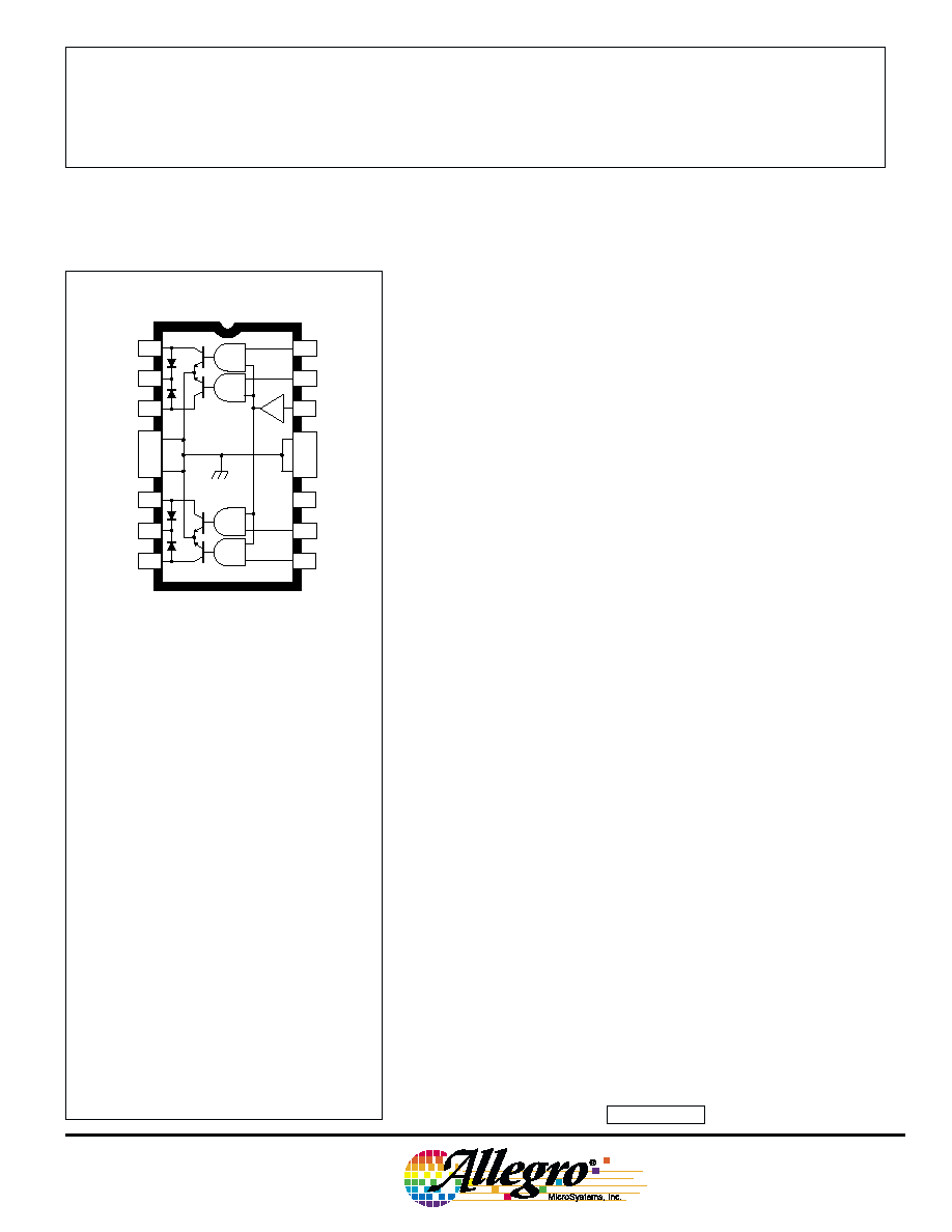
FUNCTIONAL BLOCK DIAGRAM
(1 of 4 Channels)
UDx2549EB
50
75
100
125
150
10
6
4
2
0
ALLOWABLE PACKAGE POWER DISSIPATION IN WATTS
TEMPERATURE IN
�C
8
25
R = 6
�C/W
JT
Dwg. GP-004-1A
SUFFIX 'EB', R = 36
�C/W
JA
SUFFIX 'B', R = 43
�C/W
JA
VCC
<<1
OUT
Dwg. FP-041
N
IN N
THERMAL
LIMIT
ENABLE
K
1
2
3
4
5
6
7
8
9
10
11
12
13
14
15
16
17
18
19
20
21
22
23
24
25
26
27
28
GROUND
GROUND
GROUND
GROUND
Dwg. PP-019-1
K
NO
CONNECTION
ENABLE
SUPPLY
NC
NC
CC
V
OUT
1
OUT
2
OUT
3
OUT
4
IN
4
IN
3
IN
2
IN
1
NO
CONNECTION
K
Copyright � 1991, 1995, Allegro MicroSystems, Inc.
2549
PROTECTED
QUAD POWER DRIVER
www.allegromicro.com
Characteristic
Symbol
Test Conditions
Min.
Typ.
Max.
Units
Output Leakage Current
I
CEX
V
OUT
= 60 V, V
IN
= 0.8 V, V
EN
= 2.0 V
--
<1.0
100
�A
V
OUT
= 60 V, V
IN
= 2.0 V, V
EN
= 0.8 V
--
<1.0
100
�A
Output Sustaining Voltage
V
OUT(SUS)
I
OUT
= 100 mA, V
IN
= V
EN
= 0.8 V
40
--
--
V
Output Saturation Voltage
V
OUT(SAT)
I
OUT
= 100 mA
--
--
200
mV
I
OUT
= 400 mA
--
--
400
mV
I
OUT
= 600 mA
--
--
600
mV
Over-Current Trip
I
TRIP
--
1.0
--
A
Input Voltage
Logic 1
V
IN(1)
or V
EN(1)
2.0
--
--
V
Logic 0
V
IN(0)
or V
EN(0)
--
--
0.8
V
Input Current
Logic 1
V
IN(1)
or V
EN(1)
= 2.0 V
--
--
10
�A
Logic 0
V
IN(0)
or V
EN(0)
= 0.8 V
--
--
-10
�A
Total Supply Current
I
CC
I
OUT
= 600 mA, V
IN
* = V
EN
= 2.0 V
--
--
65
mA
All Outputs OFF
--
--
15
mA
Clamp Diode Forward Voltage
V
F
I
F
= 1.0 A
--
--
1.7
V
Clamp Diode Leakage Current
I
R
V
R
= 60 V, D
1
+ D
2
or D
3
+ D
4
--
--
50
�A
Thermal Limit
T
J
--
165
--
�C
Limits
Typical Data is for design information only.
Negative current is defined as coming out of (sourcing) the specified terminal.
As used here, -100 is defined as greater than +10 (absolute magnitude convention) and the minimum is implicitly zero.
* All inputs simultaneously, all other tests are performed with each input tested separately.
ELECTRICAL CHARACTERISTICS at T
A
= +25
�
C (prefix `UDN') or over operating
temperature range (prefix `UDK' or `UDQ'), V
CC
= 4.75 V to 5.25 V
2549
PROTECTED
QUAD POWER DRIVER
115 Northeast Cutoff, Box 15036
Worcester, Massachusetts 01615-0036 (508) 853-5000
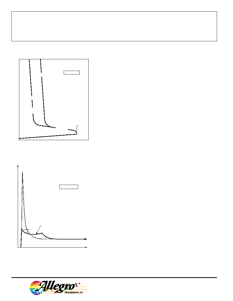
CIRCUIT DESCRIPTION AND APPLICATION
INCANDESCENT LAMP DRIVER
High incandescent lamp turn-ON/in-rush currents can contribute to
poor lamp reliability and destroy semiconductor lamp drivers. Warming
or current-limiting resistors protect both driver and lamp but use signifi-
cant power either when the lamp is OFF or when the lamp is ON,
respectively. Lamps with steady-state current ratings up to 600 mA
can be driven by these devices without the need for warming (parallel)
or current-limiting (series) resistors.
When an incandescent lamp is initially turned ON, the cold filament
is at minimum resistance and would normally allow a 10x to 12x in-rush
current. With the these drivers, during turn-ON, the high in-rush current
is sensed by the internal low-value sense resistor. Drive current to the
output stage is then diverted by the shunting transistor, and the load
current is momentarily limited to approximately 1.0 A. During this short
transition period, the output current is reduced to a value dependent on
supply voltage and filament resistance. During lamp warmup, the
filament resistance increases to its maximum value, the output stage
goes into saturation and applies maximum rated voltage to the lamp.
INDUCTIVE LOAD DRIVER
Bifilar (unipolar) stepper motors, relays, or solenoids can be driven
directly. The internal flyback diodes prevent damage to the output
transistors by suppressing the high-voltage spikes which occur when
turning OFF an inductive load. For rapid current decay (fast turn-OFF
speeds), the use of Zener diodes will raise the flyback voltage and
improve performance. However, the peak voltage must not exceed the
specified minimum sustaining voltage (V
SUPPLY
+ V
Z
+ V
F
V
OUT(SUS)
).
FAULT CONDITIONS
In the event of a shorted load, the load current will attempt to
increase. As described above, the drive current to the affected output
stage is reduced, causing the output stage to go linear, limiting the peak
output current to approximately 1 A. As the power dissipation of that
output stage increases, a thermal gradient sensing circuit will become
operational, further decreasing the drive current to the affected output
stage and reducing the output current to a value dependent on supply
voltage and load resistance.
Continuous or multiple overload conditions causing the chip tem-
perature to reach approximately 165
�C will result in an additional
reduction in output current to maintain a safe level.
If the fault condition is corrected, the output stage will return to its
normal saturated condition.
TYPICAL OUTPUT
CHARACTERISTIC
V
OUT(SAT)
Dwg. GP-013
OUTPUT VOLTAGE, V
OUT
OUTPUT CURRENT, I
OUT
T < 150
�C
T = 165
�C
J
J
JUNCTION
TEMP. LIMIT
NOT TO SCALE
TRIP
I
THERMAL
GRADIENT
SENSING
TYPICAL OUTPUT BEHAVIOR
NORMAL LAMP IN-RUSH CURRENT
TIME
THERMAL GRADIENT SENSING
CURRENT LIMIT
Dwg. WP-008
NOT TO SCALE
I
TRIP
0
LAMP CURRENT
2549
PROTECTED
QUAD POWER DRIVER
www.allegromicro.com
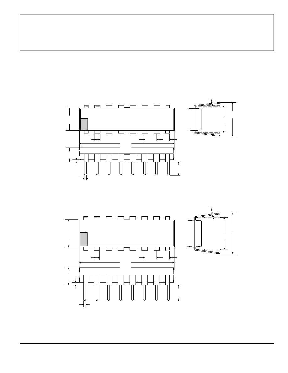
UDN2549B and UDQ2549B
Dimensions in Inches
(controlling dimensions)
Dimensions in Millimeters
(for reference only)
NOTES: 1. Exact body and lead configuration at vendor's option within limits shown.
2. Lead spacing tolerance is non-cumulative
3. Lead thickness is measured at seating plane or below.
4. Webbed lead frame. Leads 4, 5, 12, and 13 are internally one piece.
0.508
0.204
7.62
BSC
Dwg. MA-001-17A mm
10.92
MAX
16
1
8
7.11
6.10
5.33
MAX
1.77
1.15
0.39
MIN
0.558
0.356
2.54
BSC
0.13
MIN
3.81
2.93
9
19.68
18.67
NOTE 4
0.020
0.008
0.300
BSC
Dwg. MA-001-17A in
0.430
MAX
16
1
8
0.280
0.240
0.210
MAX
0.070
0.045
0.015
MIN
0.022
0.014
0.100
BSC
0.005
MIN
0.150
0.115
9
0.775
0.735
NOTE 4